You are currently viewing SemiWiki as a guest which gives you limited access to the site. To view blog comments and experience other SemiWiki features you must be a registered member. Registration is fast, simple, and absolutely free so please,
join our community today!
This was my 30[SUP]th[/SUP] DAC and the second most memorable. The most memorable was my second DAC (1985) in Las Vegas with my new bride. We had a romantic evening ending with ice cream sundaes at midnight that we still talk about. This year SemiWiki had Dr. Paul McLellan, Dr. Eric Esteve, Daniel Payne, Don Dingee, Randy Smith, and… Read More
Once upon a time, designing a product with a first generation SoC on board, we were trying to use two different I/O peripherals simultaneously. Seemed simple enough, but things just flat out didn’t work. After days spent on RTFM (re-reading the fine manual), we found ourselves at the absolute last resort: ask our FAE.
After about… Read More
There’s never a dull moment in the foundry race to offer FinFET processes that enable leading-edge SoC design. Today I attended a webinar hosted by Samsung and Synopsys on how to enable 14nm FinFET design. The two speakers were Dr. Kuang-Kuo Lin from Samsung and Dr. Henry Sheng from Synopsys.
Dr. Kuang-Kuo Lin, Samsung
Dr.… Read More
Funny story, @ #49DAC I saw Aart with a very relaxed look on his face looking at the exhibit hall and in my mind he was thinking, “Mine, all mine!” But I digress……. Synopsys is the #1 EDA company for a reason and here is the supporting data for that hypothesis:
Synopsys is committed to accelerating Innovation… Read More
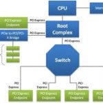
PCI Express 3.0 specification is 1000 pages long. Most of us, and most of the designers integrating PCIe gen-3 into their latest ASIC, FPGA or system will probably never read it completely, or even open it. In fact, they don’t need to read it completely, but they should care about one point, whether they buy an ASSP or a PCIe design IP:… Read More
Designing at the 20nm node is harder than at 28nm, mostly because of the lithography and process variability challenges that in turn require changes to EDA tools and mask making. The attraction of 20nm design is realizing SoCs with 20 billion transistors. Saleem Haider from Synopsys spoke with me last week to review how Synopsys… Read More
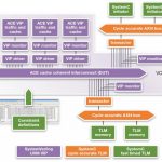
I met Mike Sanie around DVCon time and planned to write a blog about the one year anniversary of Synopsys Discovery VIP which was announced during Aart’s keynote at DVCon in 2012. Eric covered it for SemiWiki here. But Synopsys had other stuff they wanted me to blog about and so it is a couple of months late. The 14th month anniversary… Read More
… is now 8 years old, and the money paid for this 10 engineers start-up was considered, at that time, as a “bingo” for Cascade’s funders: “In October 2004, the Company completed the acquisition of Cascade Semiconductor Solutions, Inc. (Cascade) for total upfront consideration of $15.8 million and contingent consideration of … Read More
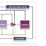
The burgeoning need of high density of electronic content on a single chip, thereby necessitating critical PPA (Power, Performance, Area) optimization, has pushed the technology node below 0.1 micron where static power becomes equally relevant as dynamic power. Moreover, multiple power rails run through the circuit at different… Read More
Cliff Hou of TSMC gave the keynote today at SNUG on Collaborate to Innovate: a Foundry’s Perspective. Starting around 45nm the way that a foundry has to work with its ecosystem fundamentally changed. Up until then, each process generation was similar enough to the previous one, apart obviously from size, that it could be … Read More