By Philippe Flatresse, Bich-Yen Nguyen, Rainer Lutz of SOITEC
I. Introduction
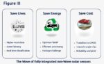
Automotive radar is a key enabler for the development of advanced driver assistance systems (ADAS) and autonomous vehicles. The use of radar allows vehicles to sense their environment and make decisions based on that information, enhancing… Read More