We spend an inordinate amount of energy tracking the big chip – the application processor – in a mobile device. As we’ve seen this space is coming down to a handful of players. A more interesting competition is heating up around the APU for the rest of chips needed to make a phone.… Read More

Tag: mems
IMEC Technology Forum at SEMICON – Coventor could save you billions!

The development of leading edge semiconductor technology is incredibly expensive, with estimates ranging from a few to several billion dollars for new nodes. The time to develop a leading edge process is also a critical competitive issue with some of the largest opportunities awarded based on who is first to yield on a new node.… Read More
LETI Day 2016 : Security in Lyon, Sensor at Semicon West on July 12th
It was the very first time I attended the LETI days, even if I know the research center for many years. LETI was created in the 60’s, as the subsidiary of the CEA (France agency in charge of Atomic Energy) in charge of Microelectronic. Now, for more than 50 years, 2000 research engineers are working to develop technologies, systems … Read More
Join the Multi-die IC session on April 21 at EDPS 2016 in Monterey, CA
Following Moore’s Law down to 10 or even 7 nm labeled feature size demands US $ hundreds of millions of up-front investment, a very large design team and two or more years of development time. These parameters suggest that it only makes sense for very high volume applications to continue on the shrink path to increase SoCs’ functionalities.… Read More
A Real Engineering Challenge – Artificial Red Blood Cells
When you’re thinking about “what can we do next”, you can think big or you can think small – very, very small. Robert Freitas at the Institute for Molecular Manufacturing (IMM) has such an idea – artificial red blood cells (RBCs). These would be nano-machines which could augment the oxygen and carbon dioxide carrying capacity of … Read More
5nm Chips? Yes, but When?
For any invention, technical proof of concept or prototyping happens years ahead of the invention being infused into actual products. When we talk about 5nm chip manufacturing, a test chip was already prototyped in last October, thanks to Cadence and Imec. Details about this chip can be found in a blog at Semiwiki (link is given … Read More
ARM on Moore’s Law at 50: Are we planning for retirement?
On Monday morning on December 7, 2016 Greg Yeric of Arm gave an excellent and wide ranging plenary talk at IEDM entitled “Moore’s Law at 50: Are we planning for retirement?”. You can download Greg’s slide deck here.… Read More
Mass customization coming to MEMS?
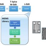
With the industry abuzz about the Apple purchase of a Maxim Integrated fab as a potential R&D facility for MEMS design, it begs the question: is creating a MEMS device that easy?
MEMS technology is approaching the same fork in the road where digital design encountered LSI four decades earlier. … Read More
Coventor prepping MEMS for CMOS integration
About 11 months ago, I wrote a piece titled “Money for data and your MEMS for free.” In that, I took on the thinking that TSMC is just going to ride into town, fab trillions of IoT sensors, and they all will be 2.6 cents ten years from now. Good headline, but the technology and economics are not that simple. This may be the semiconductor … Read More
The Internet of Sensors

The internet of things (IoT) has a number of key attributes: low power, security, connectivity. But almost every IoT application involves sensors of one sort or another. The visual sensors are built using CCD arrays, they are basically low-resolution cameras, but the mechanical ones are typically built using MEMS technology.… Read More