You are currently viewing SemiWiki as a guest which gives you limited access to the site. To view blog comments and experience other SemiWiki features you must be a registered member. Registration is fast, simple, and absolutely free so please,
join our community today!
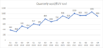
At the 2023 SPIE Advanced Lithography and Patterning conference, ASML presented an update on its EUV lithography systems in the field [1]. The EUV wafer exposure output was presented and is shown below in table form:
From this information, we can attempt to extract and assess the EUV wafer output per quarter. First, since there … Read More
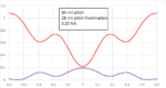
Current 1a-DRAM and 5/4nm foundry nodes have minimum pitches in the 28 nm pitch range. The actual 28 nm pitch patterns are one-dimensional active area fins (for both DRAM and foundry) as well as one-dimensional lower metal lines (in the case of foundry). One can imagine that, for a two-dimensional routing pattern, both horizontal… Read More
Masks have always been an essential part of the lithography process in the semiconductor industry. With the smallest printed features already being subwavelength for both DUV and EUV cases at the bleeding edge, mask patterns play a more crucial role than ever. Moreover, in the case of EUV lithography, throughput is a concern, … Read More
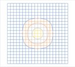
The many idiosyncrasies of EUV lithography affect the resolution that can actually be realized. One which still does not get as much attention as it should is the cross-slit pupil rotation [1-3]. This is a fundamental consequence of using rotational symmetry in ring-field optical systems to control aberrations in reflective… Read More
-Business will “drift down” over the course of 2023
-Not just memory is weak- China issue, foundry/logic slowing
-March guide worse than expected (Like Lam)
-Backlog likely saw push outs & cancelations but still long
Good quarter but weak guide
Much as we saw with Lam, KLA reported a beat on the December quarter… Read More
-Demand far exceeds supply & much longer than any downturn
-Full speed ahead-$40B in solid backlog provides great comfort
-ASP increase shows strength- China is non issue
-In a completely different league than other equipment makers
Reports a good beat & Guide
Revenues were Euro6.4B with system sales making up Euro4.7B… Read More
Stochastic defects in EUV lithography have been studied over the last few years. For years, the Poisson noise from the low photon density of EUV had been suspected [1,2]. EUV distinguishes itself from DUV lithography with secondary electrons functioning as intermediary agents in generating reactions in the resist. Therefore,… Read More
It has recently been revealed that the N5 node from TSMC has a minimum gate pitch of 51 nm [1,2] with a channel length as small as 6 nm [2]. Such a tight channel length entails tight CD control in the patterning process, well under 0.5 nm. What are the possible lithography scenarios?
Blur Limitations for EUV Exposure
A state-of-the-art
…
Read More
There is growing awareness that EUV lithography is actually an imaging technique that heavily depends on the distribution of secondary electrons in the resist layer [1-5]. The stochastic aspects should be traced not only to the discrete number of photons absorbed but also the electrons that are subsequently released. The electron… Read More
To the general public, EUV lithography’s resolution can be traced back to its short wavelengths (13.2-13.8 nm), but the true printed resolution has always been affected by the stochastic behavior of the electrons released by EUV absorption [1-5].
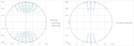
A 0.33 NA EUV system is expected to have a diffraction-limited point spread… Read More