You are currently viewing SemiWiki as a guest which gives you limited access to the site. To view blog comments and experience other SemiWiki features you must be a registered member. Registration is fast, simple, and absolutely free so please,
join our community today!
Engineers are always looking to improve the efficiency of how they work, but don’t want to sacrifice accuracy in the process. This is true in the world of semiconductor process development, where traditional build-and-test cycles are both time and resource intensive. But what if there was a way to do certain steps in a ‘virtual’… Read More
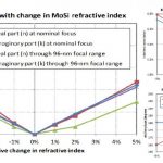
Let’s start with the bottom line: in 14nm processes, errors which have typically been little more than noise with respect to photomask critical dimension (CD) control targets at larger process nodes are about to become very significant, even out of control if not accounted for.… Read More
Round #1 was here.
In the EUV corner were Stefan Wurm of Sematech (working on mask issues mostly) and Skip Miller of ASML who are the only company making EUV steppers (and light sources, they acquired Cymer).
You may know that the biggest issue in EUV is getting the source brightness to have high enough energy that an EUV stepper has … Read More
If you want to know the state of play in lithography, there is no better place than the special session on lithography at Semicon West. This year was no exception. The session was given the punchy title Still a tale of 2 paths: multi-patterning lithography at 20nm and below: EUVL source and infrastructure progress.
In the blue corner… Read More
Cutting the Key to 14nm Lithographyby Beth Martin on 04-08-2013 at 2:30 pmCategories: EDA, Siemens EDA
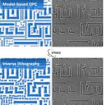
It appears that immersion lithography is now the plan of record for manufacturing ICs at 14nm. How is it possible to use 193nm wavelength light at 14nm? How can we provide the process window to pattern the such tight pitches? The secret lies in computational lithography. For 20nm, the two key innovations in computational lithography… Read More
I used my secret powers (being a blogger will get you a press pass) to go to the first day of the SPIE conference on advanced lithography a couple of weeks ago. Everything that happens to with process nodes seems to be driven by lithography, and everything that happens in EDA is driven by semiconductor process. It is the place to find … Read More
As you know, I’ve been a bit of a bear about what is happening to wafer costs at 20nm and below. At the Common Platform Technology Forum last week there were a number of people talking about this in presentations and at Harvey Jones’s “fireside chat”.
At the press lunch I asked about this. There are obviously… Read More
Thisblog with a chart showing that the cost of given functionality on a chip is no longer going to fall is, I think, one of the most-read I’ve ever written on Semiwiki. It is actually derived from data nVidia presented about TSMC, so at some level perhaps it is two alpha males circling each other preparing for a fight. Or, in this… Read More
At Semicon, Ben Rathsack of Tokyo Electron America talked about directed self assembly (DSA) at the standing-room only lithography morning. So what is it? Self assembly involves taking two monomers that don’t mix and letting them polymerise (so like styrene forming polystyrene). Since they won’t mix they will … Read More
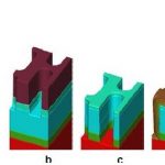
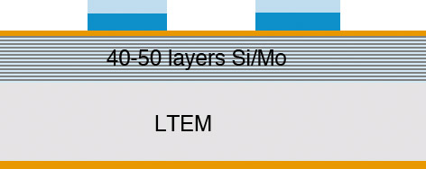
EUV Masksby Paul McLellan on 07-17-2012 at 11:00 pmCategories: Uncategorized
This is really the second part to this blog about the challenges of EUV lithography. The next speaker was Franklin Kalk who is CTO of Toppan Photomasks. He too emphasized that we can make almost arbitrarily small features but more and more masks are required (not, that I suspect, he would complain being in the mask business). For EUV… Read More