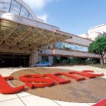
TSMC has a lot of capacity. Not just that, it has a lot more under construction. It currently has 3 300mm Gigafabs, fabs 12,14 and 15 (there doesn’t seem to be a 13). This morning, Dr Wang, who is TSMC’s VP of 300mm operations told us about the expansion plans. Currently fab 15 phase 3 and 4, and fab 12 phase 3 are to be ramped… Read More
Tag: foundry
TSMC Tapes Out First 64-bit ARM
TSMC announced today that together with ARM they have taped out the first ARM Cortex-A57 64-bit processor on TSMC’s 16nm FinFET technology. The two companies cooperated in the implementation from RTL to tape-out over six months using ARM physical IP, TSMC memory macros, and a commercial 16nm FinFET tool chain enabled by… Read More
A Brief History of the Foundry Industry, part 2
Part 1 here.
The line between fabless semiconductor companies and IDMs has blurred over the last decade. Back in the 1990s, most IDMs manufactured most of their own product, perhaps using a foundry for a small percentage of additional capacity when required. But their own manufacturing was competitive, both in terms of the capacity… Read More
A Brief History of the Foundry Industry, part 1
The fundamental economics of the semiconductor industry are summed up in the phrase “fill the fab.” Building a fab is a major investment. With a lifetime of just a few years, the costs of owning a fab are dominated by depreciation of the fixed capital assets (the building, the air and water purification equipment, the manufacturing… Read More
Intel’s x86 – Foundry Breakup Comes into View
The announcement by Intel during their January earnings call that they were going to hike Capex in 2013 over 2012 left many folks scrambling as to the reasons and the what-the hecks? Here was a company that was exiting 2012 with 50% utilization of their advanced 22nm process and yet signaling more building was to come. Furthermore,… Read More
Notes from Common Platform: Collaborate or Die
FinFETs are hot, carbon nanotubes are cool, and collaboration is the key to continued semiconductor scaling. These were the main messages at the 2013 Common Platform Technology Forum in Santa Clara.
The collaboration message ran through most presenations, like the afternoon talk by Subi Kengeri of GLOBALFOUNDRIES and Joe Sawicki… Read More
TSMC ♥ Oasys
Oasys has joined the TSMC Soft-IP Alliance Program. This means that TSMC IP partners have access to a new RTL exploration tool to improve QoR and reduce the iterations needed for design closure. In modern process nodes, RTL engineers implementing complex IP cores for graphics, networking, and mobile computing are struggling … Read More
A Brief History of Semiconductors: the Foundry Transition
A modern fab can cost as much as $10B dollars. That’s billion with a B. Since it has a lifetime of perhaps 5 years, owning a fab costs around $50 per second and that’s before you buy any silicon or chemicals or design any chips. Obviously anyone owning a fab had better be planning on making and selling a lot of chips if they are going to make… Read More
SemiWiki.com Analytics Exposed 2012
About 4 years ago some of my semiconductor cohorts urged me to blog. “Hey Dan, you’re a funny guy, write about EDA and IP, make us laugh!” Of course what I think is funny most people think is snarky, which is a nice word for being a smart ass. The traditional semiconductor press was crumbling, the non traditional EDA websites were outdated,… Read More
Smart mobile SoCs: Intel
Talk about an unusual position. Intel finds themselves very much currently outside when it comes to mobile SoCs for phones and tablets. After several attempts at soul-searching and a true understanding of the term “low-power” (not meaning 3W, but instead < 1W), they finally have a part – in the form of “Medfield”, aka the Atom… Read More


