– SPIE EUV & Photomask conference well attended with great talks
– Chip industry focused on next gen High NA EUV & what it impacts
– Do big chips=big masks? Another Actinic tool?
– AI & chip tools, a game changer- China pre-empting more sanctions

Tag: euv
Micron Chip & Memory Down Cycle – It Ain’t Over Til it’s Over Maybe Longer and Deeper

- The memory down cycle is longer/deeper than many thought
- The recovery will be slower than past cycles- a “U” rather than “V”
- AI & new apps don’t make up for macro weakness
- Negative for overall semis & equip- Could China extend downcycle?
Micron report suggests a longer deeper down cycle
… Read MoreHas U.S. already lost Chip war to China? Is Taiwan’s silicon shield a liability?
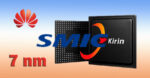
- Huawei’s 7NM chip? This wasn’t supposed to happen
- Are Chips a weapon for U.S. or China? Role reversal?
- Will Taiwan turn from protected asset to unwanted liability?
- Are sanctions so porous that US has already lost to China?
While EUV is critical to advanced chips there are workarounds
Many people either thought or assumed… Read More
Stochastic Model for Acid Diffusion in DUV Chemically Amplified Resists
Recent articles have focused much effort on studying the stochastic behavior of secondary electron exposure of EUV resists [1-4]. Here, we consider the implications of extending similar treatments to DUV lithography.
Basic Model Setup
As before, the model uses pixel-by-pixel calculations of absorbed photon dose, followed… Read More
Modeling EUV Stochastic Defects with Secondary Electron Blur
Extreme ultraviolet (EUV) lithography is often represented as benefiting from the 13.5 nm wavelength (actually it is a range of wavelengths, mostly ~13.2-13.8 nm), when actually it works through the action of secondary electrons, electrons released by photoelectrons which are themselves released from ionization by absorbed… Read More
Enhanced Stochastic Imaging in High-NA EUV Lithography
High-NA EUV lithography is the anticipated new lithography technology to be introduced for the 2nm node. Essentially, it replaces the 0.33 numerical aperture of current EUV systems with a higher 0.55 numerical aperture (NA). This allows the projection of smaller spot sizes and smaller pitches, roughly 60% smaller compared … Read More
ASML Update SEMICON West 2023
At SEMICON West I had a chance to catch up with Mike Lercel of ASML. In this article I am going to combine ASML presentation material from the SPIE Advanced Lithography Conference, Mike’s SEMICON presentation, my discussions with Mike at SEMICON and a few items from ASML’s recent earnings call.
DUV
ASML continues to improve DUV systems.… Read More
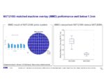
Assessing EUV Wafer Output: 2019-2022
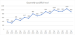
At the 2023 SPIE Advanced Lithography and Patterning conference, ASML presented an update on its EUV lithography systems in the field [1]. The EUV wafer exposure output was presented and is shown below in table form:
From this information, we can attempt to extract and assess the EUV wafer output per quarter. First, since there … Read More
Intel Internal Foundry Model Webinar
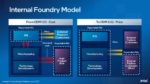
Intel held a webinar today to discuss their IDM2.0 internal foundry model. On the call were Dave Zinsner Executive Vice President and Chief Financial Officer and Jason Grebe Corporate Vice President and General Manager of the Corporate Planning Group.
On a humorous note, the person moderating the attendee questions sounded … Read More
SPIE 2023 – imec Preparing for High-NA EUV
The SPIE Advanced Lithography Conference was held in February. I recently had the opportunity to interview Steven Scheer, vice president of advanced patterning process and materials at imec and review selected papers that imec presented.
I asked Steve what the overarching message was at SPIE this year, he said readiness for … Read More