To wrap up Semicon West, let’s go back to Monday and the imec presentations. In fact, An Steegen’s presentation titled The Semiconductor Roadmap. She covered a lot of ground, but some of her slides contain a wealth of information. Let’s look at the options for 10nm, 7nm and a little 5nm, what imec call N10, N7 and… Read More

Tag: euv
EUV Will Never Happen
I had lunch today with a guy who has to remain nameless. But he is on the edge of the semiconductor lithography thing. He told me EUV will never happen. Of course lots of people have said that. Me for one. But he said everyone knows it. The investment community, the foundries, everyone. Intel put money into ASML in the hopes that it would… Read More
EUV Slips a Year Per Year…Or More

I was at EDPS in Monterey the last couple of days. It is one of the most interesting conferences to attend. Go next year since you already missed it this year. It is not big but the quality of the content is high. Historically the dinner in the middle is in the Monterey Yacht Club and there is a keynote speech. A few years ago it was me but this… Read More
450mm Delayed and Other SPIE News
Last week I attended the SPIE Advanced Technology Conference. There were a lot of interesting papers and as is always the case at these conferences, there was a lot of interesting things to learn from talking to other attendees on the conference floor.
The first interesting information from the conference floor was that 450mm is… Read More
The State of 450mm Wafers. And Intel Gossip
Paul Farrar, the General Manager of the Global 450mm Consortium (G450C) presented at the SEMI ISS conference today. What is G450C, it is a public-private consortium to develop a cost-effective 450mm wafer fabrication infrastructure, develop equipment prototypes and coordinate the industry move to 450mm. It is located in Albany… Read More
Technology Challenges: Intel, IBM, Xilinx, GlobalFoundries, IMEC
I spent the day at the SEMI Industry Strategy Symposium in Half Moon Bay. The early part of the day was devoted to technology challenges. Obviously everyone did not say exactly the same things, and had a little bit of a different spin depending on what business they are in. But there was a lot of commonality between Intel, IBM, Xilinx… Read More
Lithography: Future Technologies

The first part of Lars Liebmann’s ICCAD keynote about lithography was on the changes in lithography that have to us to where we are today. In some ways it was an explanation of why we have the odd design rules, double patterning etc that we have in 20nm and 16nm processes. The second part of his talk was a look forward to how we might… Read More
Semicon: Multiple Patterning vs EUV, round #2

Round #1 was here.
In the EUV corner were Stefan Wurm of Sematech (working on mask issues mostly) and Skip Miller of ASML who are the only company making EUV steppers (and light sources, they acquired Cymer).
You may know that the biggest issue in EUV is getting the source brightness to have high enough energy that an EUV stepper has … Read More
Semicon: Multiple Patterning vs EUV, round #1
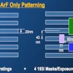
If you want to know the state of play in lithography, there is no better place than the special session on lithography at Semicon West. This year was no exception. The session was given the punchy title Still a tale of 2 paths: multi-patterning lithography at 20nm and below: EUVL source and infrastructure progress.
In the blue corner… Read More
SEMICON West: My Top Picks
I will be at Semicon West from 9th to 11th July in Moscone, San Francisco. Of course there are lots of interesting sessions but here are two that I think are especially important to get a good impression of the way things are going in the future from experts. The two most interesting questions about the future are what comes after 14nm,… Read More