You are currently viewing SemiWiki as a guest which gives you limited access to the site. To view blog comments and experience other SemiWiki features you must be a registered member. Registration is fast, simple, and absolutely free so please,
join our community today!
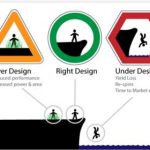
Solido Design Automation is rapidly making a name for itself in EDA. Amit Gupta is founder and CEO of Solido Design Automation, based in Saskatoon, Canada. You should also know that Solido is one of the founding members of SemiWiki.com. In the last six years we have published 44 Solido related blogs that have racked up more than 200,000… Read More
Fascinated by computers at a very young age, Peter got his degree in Computer Science and was brought to the Bay Area via AIESEC Berkeley’s student exchange program to write his thesis. He has now more than 15 years of professional experience in software engineering, large scale systems architecture and data center engineering… Read More
Magwel CEO Dündar Dumlugöl is well known from his days at Cadence, where I first met him, and for his more recent tenure at Magwel. At Cadence he led the team that first developed Spectre. He has come a long way from the start of his career at IMEC in Belgium. He and I had a chance to have a conversation recently where he offered insights … Read More
This interview originally appeared as the foreword to our book “Prototypical: The Emergence of FPGA-based Prototyping for SoC Design” but I thought it would be worth publishing for those of you who have not downloaded it yet. I also wanted to mention that our friends at S2C are currently offering a 50% discount on the… Read More
As a longtime EDA professional this really made my day. At a time where emerging EDA companies struggle for public validation, it warms my heart to see some very public recognition for an EDA job well done.
Deloitte, a leading Canadian professional financial services firm, announced the winners of their Technology Fast 50 program… Read More
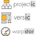
It has been interesting to watch Methodics transform from an EDA company with their VersIC design management product to Life Cycle Management with ProjectIC, and now a Systems Company with WarpStor. Methodics was founded in 2006 by 2 ex-Cadence experts in the Custom IC design tools space, Simon Butler and Fergus Slorach. Today… Read More
This week Cadence Design, Lumerical Solutions and PhoeniX Software hosted a two-day photonic summit and workshop. The first day had nearly 100 registered participants and featured industry leaders from Global Foundries, UCSB, MIT, Hewlett Packard Enterprise, General Electric, Boeing, Rockley Photonics, and Juniper Networks… Read More
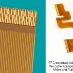
The three F’s of electronic product development are: form, fit, and function. Although the F/F/F assessment typically refers to the selection of the right component, it most definitely also refers to the selection of the proper cabling between assemblies. The requirements for cables are varied, and demanding: ability… Read More
Do not lose sleep worrying that your integrated circuits might fail during EOS/ESD events. Join us for the 38th annual EOS/ESD Symposium in Anaheim, CA in September. Experts on the field will address the latest research on EOS and ESD in the rapidly changing world of electronics.
As electronics continue to become commonplace in… Read More
At the #53DAC earlier this month held in Austin, Texas I met up with Renee Donkers, the founder of Fractal Technologies. His company has been focused on improving the quality of semiconductor IP cells through the use of automated checking software. The highest area of growth in EDA as measured by the ESD Alliance is in the reusable… Read More