You are currently viewing SemiWiki as a guest which gives you limited access to the site. To view blog comments and experience other SemiWiki features you must be a registered member. Registration is fast, simple, and absolutely free so please,
join our community today!
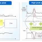
Power has become the strongest driver of semiconductor design today, more important than area, more important than timing. Whether the device is handheld, like a wireless phone, or tethered, like a router, complex power and energy requirements must be met. Shrinking geometries continue to impose new challenges as power management… Read More
Virtual platforms have been an area that has some powerful value propositions for both architectural analysis and for software development. But the fundamental weakness has been the modeling problem. People want fast and accurate models but this turns out to be a choice.
The first issue is that there is an unavoidable tradeoff… Read More
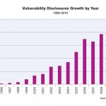
The IBM X-ForceTrend and Risk Report reveals how 2010 was a pivotal year for internet security as networks faced increasingly sophisticated attacks from malicious sources around the world. The X-Force reportedly monitors 13 billion real-time security events every day (150,000 events per second) and has seen an increase in … Read More
Inroduction
In the early days we made paper plots of an IC layout then measured the width and length of interconnect segments with a ruler to add up all of the squares, then multiplied by the resistance per square. It was tedious, error prone and took way too much time, but we were rewarded with accurate parasitic values for our SPICE… Read More
Yesterday at the Globalpress electronic summit Andrew gave an overview of the Apache product line, carefully avoiding saying anything he cannot due to the filing of Apache’s S-1. From a financial point of view the company has had 8 years of consecutive growth, is profitable since 2008, and has no debt. During 2010 when the… Read More
In part I of this series, we looked at the history of lithography process models, starting in 1976. Some technologies born in that era, like the Concorde and the space shuttle, came to the end of their roads. Others did indeed grow and develop, such as the technologies for mobile computing and home entertainment. And lithography … Read More
Apache Design Solutions today filed their S-1 with the SEC in preparation for its initial public offering (IPO). This is a big deal since there hasn’t been an IPO of an EDA company for may years (Magma was the last 10 years ago). As a private company they have not had to reveal their financials until now.
It turns out that they did… Read More
Last week I met with Joseph Davis, Ph.D. at Mentor Graphics in Wilsonville, Oregon to learn about a new product designed for full-custom IC layout designers to improve productivity.
The traditional flow for full-custom IC layout designers has been nearly unchanged for decades:
- Read a schematic or use Schematic Driven Layout
…
Read More
The 17[SUP]th[/SUP] Annual TSMC Technology Symposium will be held in San Jose California on April 5[SUP]th[/SUP], 2011. Dr. Morris Chang will again be the keynote speaker. The theme this year is “Trusted Technology and Capacity Provider”and I think it’s important to not only hear what people are saying but also understand why… Read More
This is just another blog about Carl Icahn and his quest to conquer EDA, when in fact EDA is conquering him. It includes highlights from my dinner with Mentor Graphics and Physicist Brian Greene, the Mentor Q4 conference call, and meeting Mentor CEO Wally Rhines at DvCon 2011.
It wasn’t just the free food this time, dinner with Brian… Read More