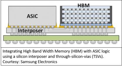
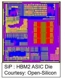
High Bandwidth Memory (HBM) systems have been successfully used for some time now in the network switching and high-performance computing (HPC) spaces. Now, adding fuel to the HBM fire, there is another market that shares similar system requirements as HPC and that is Artificial Intelligence (AI), especially AI systems doing… Read More
Tag: 2.5d
Advanced ASICs – It Takes an Ecosystem
I remember the days of the IDM (integrated device manufacturer). For me, it was RCA, where I worked for 15 years as the company changed from RCA to GE and then ultimately to Harris Semiconductor. It’s a bit of a cliché, but life was simpler then, from a customer point of view at least. RCA did it all. We designed all the IP, did the physical… Read More
Navigating the System-in-a-Package Manufacturing Ecosystem
Being an old ASIC physical design guy, I tend to think of ASICs from a “bond-pads-in” perspective. This week however, I had a very eye-opening discussion with Dan Leung, Director of Packaging and Assembly for Open-Silicon, that totally changed my perspective. While I had been exposed many times to the concept of systems-in-a-package… Read More
Memories for the Internet
In 1969 the Internet was born at UCLA when a computer there sent a message to a computer at Stanford. By 1975, there were 57 computers on the ‘internet’. Interestingly in the early seventies I actually used the original Xerox Sigma 7 connected to the internet in Boelter Hall at UCLA. A similar vintage computer is now in this room commemorating… Read More
Samsung Should Just Buy eSilicon Already!
As you all know I’m a big fan of the ASIC business dating back to the start of the fabless semiconductor transformation where anybody could send a design spec to an ASIC company and get a chip back. The ASIC business model also started the smart phone revolution when Samsung built the first Apple SoCs for the iPhones and iPads.
Today … Read More
Another Live Event at Samsung!
Last week Samsung hosted the GSA Silicon Valley “State of the Industry” Meet-up which was well attended by the semiconductor elite, myself included. The agenda started with an update on the semiconductor industry outlook followed by deep dives into Automotive, IoT, Artificial Intelligence, and Cybersecurity all of which are… Read More
“Thinking Outside the Chip”
While pushing Moore’s Law’s boundaries in the world of 2D packaging, companies are starting to explore nontraditional approaches towards designing integrated circuit chips. 2D packaging is currently the most used method in designing chips in the industry, and while it leads in efficiency of power and performance, it lacks … Read More
Pathfinding to an Optimal Chip/Package/Board Implementation
A new term has entered the vernacular of electronic design engineering — pathfinding. The complexity of the functionality to be integrated and the myriad of chip, package, and board technologies available make the implementation decision a daunting task. Pathfinding refers to the method by which the design space of technology… Read More
GlobalFoundries and ARM
GlobalFoundries had several interesting things at the ARM TechCon last week. Firstly, GlobalFoundries won the best in show award in the chip design category recognizing the best-in-class technologies introduced since the last TechCon.
Earlier in the summer GlobalFoundries and ARM announced the ARM Cortex-A12 processor,… Read More
Emerging Trend – Choose DRAM as per Your Design Need
Lately I was studying about new innovations in memory world such as ReRAM and Memristor. As DRAM (although it has become a commodity) has found its extensive use in mobile, PC, tablet and so on, that was an inclination too to know more about. While reviewing Cadence’s offering in memory subsystems, I came across this whitepaperwhich… Read More


