This is the 15th anniversary of the TSMC Open Innovation Platform (OIP). The OIP Ecosystem Forum will kick off on September 27th in Santa Clara, California and continue around the world for the next two months in person and on-line in North America, Europe, China, Japan, Taiwan, and Israel. These are THE most attended semiconductor ecosystem networking events! I hope to see you there!
For more information check TSMC.com.
Growing up in Silicon Valley with a 40 year career in the semiconductor industry/ecosystem has been an amazing experience. Working with the most intelligent people around the world, solving some of the most complex problems, and seeing the fruits of our labor change the world, there is nothing like being a semiconductor professional.
This next passage is an updated chapter from our book “Fabless: The transformation of the Semiconductor Industry“. It captures the OIP backstory quite nicely but there is just one thing I would like to add. The amount of money invested by TSMC and the OIP partners in the ecosystem every year is billions of dollars. The total ecosystem investment is most certainly more than a trillion dollars and I must say we certainly are getting our money’s worth, absolutely.
In Their Own Words: TSMC and Open Innovation Platform
TSMC, the largest and most influential pure-play foundry,
has many fascinating stories to tell. In this section, TSMC
covers some of their basic history, and explains how creating
an ecosystem of partners has been key to their success, and to
the growth of the semiconductor industry.
The history of TSMC and its Open Innovation Platform (OIP)® is, like almost everything in semiconductors, driven by the economics of semiconductor manufacturing. Of course, ICs started 50 years ago at Fairchild, very close to where Google is headquartered today (these things go in circles). The planarization approach, whereby a wafer (just 1” originally) went through each process step as a whole, led to mass production. Other companies such as Intel, National, Texas Instruments and AMD soon followed and started the era of the Integrated Device Manufacturer (although we didn’t call them that back then, we just called them semiconductor companies).
The next step was the invention of ASICs with LSI Logic and VLSI Technology as the pioneers. This was the first step of separating design from manufacturing. Although the physical design was still done by the semiconductor company, the concept was executed by the system company. Perhaps the most important aspect of this change was not that part of the design was done at the system company, but rather the idea for the design and the responsibility for using it to build a successful business rested with the system company, whereas IDMs still had the “if we build it they will come” approach, with a catalog of standard parts.
In 1987, TSMC was founded and the separation between manufacture and design was complete. One missing piece of the puzzle was good physical design tools. Fortunately, Cadence was created in 1988 from the merger of SDA and ECAD (and soon after, Tangent). Cadence was the only supplier of design tools for physical place and route at the time. It was now possible for a system company to buy design tools, design their own chip and have TSMC manufacture it. The system company was completely responsible for the concept, the design, and selling the end-product (either the chip itself or a system containing it). TSMC was completely responsible for the manufacturing (usually including test, packaging and logistics too).
At the time, the interface between the foundry and the design group was fairly simple. The foundry would produce design rules and SPICE parameters for the designers; the design would be given back to the foundry as a GDSII file and a test program. Basic standard cells were required, and these were available on the open market from companies like Artisan, or some groups would design their own. Eventually TSMC would supply standard cells, either designed in-house or from Artisan or other library vendors (bearing an underlining royalty model transparent to end users). However, as manufacturing complexity grew, the gap between manufacturing and design grew too. This caused a big problem for TSMC: there was a lag from when TSMC wanted to get designs into high volume manufacturing and when the design groups were ready to tape out. Since a huge part of the cost of a fab is depreciation on the building and the equipment, which is largely fixed, this was a problem that needed to be addressed.
At 65 nm TSMC started the Open Innovation Platform (OIP) program. It began at a relatively small scale but from 65 nm to 40 nm to 28 nm the amount of manpower involved went up by a factor of 7. By 16 nm FinFET, half of the design effort is IP qualification and physical design because IP is used so extensively in modern SoCs. OIP actively collaborated with EDA and IP vendors early in the life-cycle of each process to ensure that design flows and critical IP were ready early. In this way, designs would tape-out just in time as the fab was starting to ramp so that the demand for wafers was well-matched with the supply.
In some ways the industry has gone a full circle, with the foundry and the design ecosystem together operating as a virtual IDM. The existence of TSMC’s OIP program further sped up disaggregation of the semiconductor supply chain. This was enabled partly by the existence of a healthy EDA industry and an increasingly healthy IP industry. As chip designs had grown more complex and entered the SoC era, the amount of IP on each chip was beyond the capability or the desire of each design group to create. But, especially in a new process, EDA and IP qualification was a problem.
On the EDA side, each new process came with some new discontinuous requirements that required more than just expanding the capacity and speed of the tools to keep up with increasing design size. Strained silicon, high-K metal gate, double patterning and FinFETs each require new support in the tools and designs to drive the development and test of the innovative technology.
On the IP side, design groups increasingly wanted to focus all their efforts on parts of their chip that differentiated them from their competition, and not on re-designing standard interfaces. But that meant that IP companies needed to create the standard interfaces and have them validated in silicon much earlier than before.
The result of OIP has been to create an ecosystem of EDA and IP companies, along with TSMC’s manufacturing, to speed up innovation everywhere. Because EDA and IP groups need to start work before everything about the process is ready and stable, the OIP ecosystem requires a high level of cooperation and trust.
When TSMC was founded in 1987, it really created two industries. The first, obviously, is the foundry industry that TSMC pioneered before others entered. The second was the fabless semiconductor industry where companies did not need to invest in fabs.
The foundry/fabless model largely replaced IDMs and ASIC. An ecosystem of co-operating specialist companies innovates fast. The old model of having process, design tools and IP all integrated under one roof has largely disappeared, along with the “not invented here” syndrome that slowed progress since ideas from outside the IDMs had a tough time penetrating. Even some of the earliest IDMs from the “Real men have fabs” era have gone “fab lite” and use foundries for some of their capacity, typically at the most advanced nodes.
Legendary TSMC Chairman Morris Chang’s “Grand Alliance” is a business model innovation of which OIP is an important part, gathering all the significant players together to support customers—not just EDA and IP, but also equipment and materials suppliers, especially for high-end lithography.
Digging down another level into OIP, there are several important components that allow TSMC to coordinate the design ecosystem for their customers.
- EDA: the commercial design tool business flourished when designs got too large for hand-crafted approaches and most semiconductor companies realized they did not have the expertise or resources in-house to develop all their own tools. This was driven more strongly in the front-end with the invention of ASIC, especially gate-arrays, and then in the back end with the invention of foundries.
- IP: this used to be a niche business with a mixed reputation, but now is very important with companies like ARM, Imagination, CEVA, Cadence, and Synopsys, all carrying portfolios of important IP such as microprocessors, DDRx, Ethernet, flash memory and so on. In fact, large SoCs now contain over 50% and sometimes as much as 80%.
- Services: design services and other value-chain services calibrated with TSMC process technology helps customers maximize efficiency and profit, getting designs into high volume production rapidly.
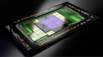
- Packaging: TSMC expanded the OIP ecosystem to include a 3D Fabric Alliance.
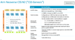
- People: More than 3,000 TSMC employees are part of OIP plus 10,000 people from the more than 100 OIP partners. The OIP now includes 50,000 titles, 43,000 tech files, and 2,800 PDKs.
Processes are continuing to get more advanced and complex, and the size of a fab that is economical also continues to increase. This means that collaboration needs to increase as the only way to both keep costs in check and ensure that all the pieces required for a successful design are ready just when they are needed.
TSMC has been building an increasingly rich ecosystem for over 30 years and feedback from partners is that they see benefits sooner and more consistently than when dealing with other foundries. Success comes from integrating usage, business models, technology and the OIP ecosystem so that everyone succeeds. There are a lot of moving parts that all have to be ready. It is not possible to design a modern SoC without design tools. More and more SoCs involve more and more 3rd party IP, and, at the heart of it all, the process and the manufacturing ramp with its associated yield learning all needs to be in place at TSMC.
Bottom line: The OIP ecosystem has been a key pillar in enabling this sea of change in the semiconductor industry.
Also Read:
How Taiwan Saved the Semiconductor Industry
Morris Chang’s Journey to Taiwan and TSMC
The First TSMC CEO James E. Dykes