One of the most common things I hear now is that the majority of the fabless semiconductor business will stay at 28nm due to the high cost of FinFETs. I wholeheartedly disagree, mainly because I have been hearing that for many years and it has yet to be proven true. The same was said about 40nm since 28nm HKMG was more expensive, which is one of the reasons why 28nm poly/SiON was introduced first.
Continue reading “Are FinFETs too Expensive for Mainstream Chips?”
Who Will Get the Next Bite of Apple Chip Business?
Recent reports have Intel displacing Qualcomm as the modem supplier and TSMC as the foundry for the next Apple A10 SoC. That is if you call this a credible report: Continue reading “Who Will Get the Next Bite of Apple Chip Business?”
Wafer-Level Chip-Scale Packaging Technology Challenges and Solutions
At the recent TSMC OIP symposium, Bill Acito from Cadence and Chin-her Chien from TSMC provided an insightful presentation on their recent collaboration, to support TSMC’s Integrated FanOut (InFO) packaging solution. The chip and package implementation environments remain quite separate. The issues uncovered in bridging that gap were subtle – the approaches that Cadence described to tackle these issues are another example of the productive alliance between TSMC and their EDA partners.
WLCSP Background
Wafer-level chip-scale packaging was introduced in the late 1990’s, and has evolved to provide an extremely high-volume, low-cost solution.
Wafer fabrication processing is used to add solder bumps to the die top surface at a pitch compatible with direct printed circuit board assembly – no additional substrate or interposer is used. A top-level thick metal redistribution layer is used to connect from pads at the die periphery to bump locations. The common terminology for this pattern is a “fan-in design”, as the RDL connections are directed internally from pads to the bump array.
[Ref: “WLCSP”, Freescale Application Note AN3846]
WLCSP surface-mount assembly is now a well-established technology – yet, the fragility of the tested-good silicon die during the subsequent dicing, (wafer-level or tape reel) pick, place, and PCB assembly steps remains a concern.
To protect the die, a backside epoxy can be applied prior to dicing. To further enhance post-assembly attach strength and reliability, an underfill resin with an appropriate coefficient of thermal expansion is injected.
A unique process can be used to provide further protection of the backside and also the four sides of the die prior to assembly – an “encapsulated” WLCSP. This process involves separating and re-placing the die on a (300mm) wafer, which will be used as a temporary carrier.
The development of this encapsulation process has also enabled a new WLCSP offering, namely a “fan-out” pad-to-bump topology.
Chip technology scaling has enabled tighter pad pitch and higher I/O counts, which necessitate a “fan-out” design style to match the less aggressively-scaled PCB pad technology. TSMC’s new InFO design enables a greater diversity of bump patterns. Indeed, it offers comparable flexibility as conventional (non-WLCSP) packaging.
Briefly, the fan-out technology starts by adding an adhesive layer to the wafer carrier. Die are (extremely accurately!) placed on this layer at a precise separation, face-down to protect the active top die surface. A molding compound is applied across the die backsides, then cured. The adhesive layer and original wafer are de-attached, resulting in a “reconstituted” wafer of fully-encapsulated die embedded in the compound:
(Source: TSMC. Molding between die highlighted in blue. WLCSP fan-out wiring to bumps extends outside the die area.)
This new structure can then be subjected to “conventional” wafer fabrication steps to complete the package:
- addition of dielectric and metal layer(s) to the die top surface
- patterning of metals and (through-molding) vias
- addition of Under Bump Metal, or UBM (optional, if the final RDL layer can be used instead)
- final dielectric and bump patterning
- dicing, with molding in place on all four sides and back
- back-grind to thin the final package
As illustrated in the figure, multi-chip and multi-layer wiring options are supported.
InFO design and verification Cadence tool flow
Cadence described the tool enhancements developed to support the InFO package. The key issue(s) arose from the “chip-like” reconstituted wafer process fabrication.
For InFO physical design, TSMC provides design rules in the familiar verification infrastructure for chip design, using a tool such as Cadence’s PVS. As an example, there are metal fill and metal density requirements associated with the fan-out metal layer(s) that are akin to existing chip design rules, a natural for PVS. (After the final package is backside-thinned, warpage is a major concern, requiring close attention to metal densities.)
Yet, InFO design is undertaken by package designers familiar with tools such as Cadence’s Allegro Package Designer or SiP Layout, not Virtuoso. As a result, the typical data representation associated with package design (Gerber 274X) needs to be replaced with GDS-II.
Continuous arcs/circles and any-angle routing need to be “vectorized” in GDS-II streamout from the packaging tools, in such a manner to be acceptable to the DRC runset – e.g., “no tiny DRC’s after vectorization”.
Viewing of PVS-generated DRC errors needs to be integrated into the package design tool environment.
Additionally, algorithms are needed to perforate wide metal into meshes. Routing algorithms for InFO were enhanced. Fan-out bump placements (“ballout”) should be optimized during co-design, both for density and to minimize the number of RDL layers required from the chip pinout.
For electrical analysis of the final design, integration of the InFO data with extraction, signal integrity, and power integrity tools (such as Cadence’s Sigrity) is required.
Cadence will be releasing an InFO design kit in partnership with TSMC, integrated with their APD and SiP products, to enable package designers to work seamlessly with (“chip design-like”) InFO WLCSP data. The bridging of these two traditionally separate domains is pretty exciting stuff.
-chipguy
Cadence Outlines Automotive Solutions at TSMC OIP Event

I used to joke that my first car could survive a nuclear war. It was a 1971 Volvo sedan (142) that was EMP proof because it had absolutely no semiconductors in the ignition system, just points, condensers and a coil. If you go back to the Model T in 1915 you will see that the “on-board electronics” were not that different. However, today’s cars have an ever increasing amount of semiconductor content. Let’s just hope there are no EMP’s anytime soon.
Automotive electronics systems now have enormous requirements for computation, bandwidth and reliability. I attended a talk by Cadence’s Charles Qi at the recent TSMC Open Innovation Platform (OIP) Forum where he outlined the major trends in this area.
By comparison to current needs, the previous bandwidth requirements were quite low. Cars have used simple networks like CAN, but increasing complexity is leading to the adoption of Ethernet standards specifically adapted to automotive needs and environments. The diagram below highlights the kinds and numbers of systems that are going to be built into cars.
As you can tell, there is audio, visual and sensor data that needs to be handled. There are strict requirements for timely delivery of certain data in automotive systems. The umbrella term for this is AVB, or Audio Video Bridging. It is broken down into a set of IEEE standards within 802.1BA. These standards address time synchronization, traffic shaping and priority queuing. Below is a diagram that lists the applicable IEEE standards for automotive communication.
Ethernet offers many advantages. It can run over twisted pair, it can carry power and it is an established standard that will continue to provide legacy support for many years. Charles outlined Cadence’s IP offerings which address the evolving Ethernet communication needs in automotive applications. Here is his slide that summarizes Cadence’s solution.
Many of the systems in the first diagram require significant processing power. Today’s systems already perform Advanced Driver Assistance (ADAS), and will be pushed even further when self driving cars arrive in earnest. Already radar based features include front collision avoidance braking, adaptive cruise control and rear collision detection. Additionally, there are vision and audio/sound based systems that will require computing power.
Cadence is positioning its Tensilica IP as a solution for automotive processing. They have a power sipping architecture that can be fine tuned to specific applications; and the development tools work to create custom compilers and libraries for many of the coding needs encountered in developing systems for emerging automotive standards.
Tensilica also offers customizable DSP cores to further accelerate automotive product development. Their IVP DSP’s are well suited for ADAS development. The IVP DSP offers VLIW and 64 way SIMD. Coming in under 300mW, they offer impressive performance with minimal power draw. One of the most interesting slides was on the problem of pedestrian detection. ADAS systems will need to do this efficiently and reliably, even if the person only shows in as small an area as 64×128 pixels.
Charles also spoke about ISO26262; we will be hearing a lot more about this in the coming years. It is a comprehensive standard for ensuring functional safety starting at the requirements phase and going through implementation. Unlike phones and fitness computers, automotive electronics play a role in life or death situations. Everything designed for automotive applications will need to comply with ISO26262. Here is a slide from Charles’ talk that gives an overview.
Well, I am still waiting for my self driving car. However, it is clear that automobiles will be competing on a lot more than looks and horsepower. In the meantime I look forward to the increased safety and possibly easier driving that things like front collision avoidance braking and adaptive cruise control will offer. For more information on Cadence IP for automotive applicationslook here at their website.
Xilinx Skips 10nm
At TSMC’s OIP Symposium recently, Xilinx announced that they would not be building products at the 10nm node. I say “announced” since I was hearing it for the first time, but maybe I just missed it before. Xilinx would go straight from the 16FF+ arrays that they have announced but not started shipping, and to the 7FF process that TSMC currently have scheduled for risk production in Q1 of 2017. TSMC already have yielding SRAM in 7nm and stated that everything is currently on-track.
See also TSMC OIP: What To Do With 20,000 Wafers Per Day although I screwed up the math and it is really over 50,000
I think that there are two reasons for doing this. The first is that TSMC is pumping out nodes very fast. Risk production for 10FF is Q4 of 2015 (which starts inext week) and so there are only 6 quarters between 10FF and 7FF if all the schedules hold. I think that makes it hard for Xilinx to get two whole families designed with some of the design work going on in parallel. It costs about $1B to create a whole family of FPGAs in a node. On the business side of things, 10nm would be a short-lived node. The leading edge customers would move to 7nm as soon as it was available so the amount of production business to generate the revenue to pay for it all and make a profit might well be too limited.
I contacted Xilinx to try and they pretty much confirmed my guess:The simple reason is that our development timelines & product cadence lined up better with 7nm introduction. TSMC has a very competitive process technology and world class foundry services and their timeline for their 7nm introduction lines up well with our needs and plans.
There have been rumors that Intel might skip 10nm too, although the recent rumors are that they will tape out a new 10nm core M processor early next year. I don’t know lf anything much that Intel has said about 7nm, either from a technology or a timing point of view.
See also Intel to Skip 10nm to Stay Ahead of TSMC and Samsung?
See also Intel 10nm delay confirmed by Tick Tock arrhythmia leak-“The Missing Tick”
That brings up the second big reason. All processes with the same number are not the same. TSMC’s 16FF process has the same metal stack (BEOL) as their 20nm process. It is their first FinFET process and so presumably they didn’t want to change too many things at once. Interestingly, Intel made the same decision the other way around at 22nm, where they had their first FinFET process (they call it TriGate) but kept the metal pitch at 80nm so it could still be single patterned. The two derivative TSMC 16nm processes, 16FF+ and 16FFC, have the same design rules and so the same 20nm metal. This limits the amount of scaling from 20nm to 16nm. There is a big difference in speed and power but not so much in density.
See also Scotten Jones’s tables in Who Will Lead at 10nm?
At 10nm Intel has a gate pitch of 55nm and a metal 1 pitch of 38nm (multiplied together gives 2101nm[SUP]2[/SUP] although I get 2090nm[SUP]2[/SUP]). TSMC at 10nm has a gate pitch of 70nm and a metal 1 pitch of 46nm, for an area of 3220nm[SUP]2[/SUP]. But perhaps more tellingly, Intel’s 14nm has a gate pitch of 70nm (same as TSMC’s 10nm) and a metal 1 pitch of 52nm, only a little looser than TSMC’s 10nm pitch of 46nm. So another reason Xilinx might skip 10nm is that it would not look good against Altera’s products in 14nm.
TSMC say that 10nm is about 50% smaller than their 16nm processes. TSMC said that 7FF will be 45% of the area of 10FF. Without any information to go on, it is still clear that Intel’s 7nm will be higher density than TSMC’s. The TSMC 7nm process will probably close to the Intel 10nm process. This is not necessarily a criticism of anyone. Intel is totally focused on bringing out server microprocessors and can read the riot act to all their designers as to how restrictive their methodology has to be and the designers have to suck it up. TSMC has to accept a much wider range of designs from a broad group of customers that they do not control in the same way.
[TABLE] style=”width: 400px”
|-
| Intel: you will do designs this way
Intel designers: but…
Intel: you will
Intel designers: OK
| TSMC: you will do designs this way
Apple engineers: no we won’t
TSMC: OK
|-
One wrinkle in all of this is also the Intel acquisition of Altera, Xilinx’s primary competitor. They seem to have been struggling to tape-out their designs in Intel’s 14nm process. If Intel is serious about using FPGAs in the datacenter, especially if they want to put the arrays on the same substrate as the processor, then they will need to get Altera’s fabric into 10nm and then 7nm hot on the heels of the server processors themselves. Xilinx’s worst nightmare would be if they produced a family of arrays in TSMC 10nm (only slightly better than Intel 14nm) and Altera got a family out in Intel’s 7nm which is a generation ahead.
So, Xilinx skipping 10nm and Altera being acquired by Intel with an opaque roadmap makes for an interesting spectator sport.
How to Build an IoT Endpoint in Three Months
It is often said that things go in big cycles. One example of this is the design and manufacturing products. People long ago used to build their own things. Think of villagers or settlers hundreds of years ago, if they needed something they would craft it themselves. Then came the industrial revolution and two things happened. One is that if you wanted something like furniture or tools you were better off buying them. The other was there was a loss of skills; people ‘forgot’ how to make things. This meant that the ability to create was concentrated in the hands of a few, and individuals had less control over what was available to them.
The maker movement has changed all that. The ability to design and build things has come full circle. Now if you want to design with 3D Printers and Arduino boards you can design a range of things, from simple everyday items to sophisticated appliances. In many ways the Internet of Things was started through this same pathway. People took low cost development systems and tools, added sensors, wireless and often servos to make a wide variety of useful things.
Semiconductor design has followed an analogous path. Early on design teams were small and they built chips that became the components of that era’s products. I remember calling on chip design companies in the late 90’s where it was literally three guys with a Sun workstation running layout software.
That era has ended and it seems that recently the only feasible way to design chips was at places like Nvidia, Intel, Freescale, Marvell, etc. They can apply design teams with hundreds of people to build their products. If you had an idea for a design and did not have the manpower, your idea went un-built.
However, things are changing again. The same market and technology forces that drove the maker movement, and pushed for standardization of building blocks, has spilled over into the internals of chip design. With the need for increased sophistication, the tools for building integrated platforms for IoT have been growing and maturing. We all know the formula by now: MCU, on board NVM, one or more radios, ultra low power, security, interfaces to sensors and a SW development environment to build user applications.
Differentiation is the key to success; product developers know they need to optimize their platform for their specific needs. ARM recently embarked on a project to test out the real world feasibility of having a small team build a custom IoT end point device in a fleeting 3 months. ARM used the TSMC Open Innovation Platform Forum in September to present their results.
ARM Engineering Director Tim Whitfield gave a comprehensive presentation on their experience. The challenge was to go from RTL to GDS in 3 months with 3 engineers. additionally, there were hard analog RF blocks that needed to be integrated. They went with the ARM mbedOS to make it easy to prototype. They also included standard interfaces like SPI and I2C for easy integration of external sensors.
ARM used their arsenal of building blocks which includes the Cortex M3, Artisan physical IP, mbedOS, Cordio BT4.2, ancillary security hardware and some TSMC IP as well. The radio was the most interesting part of the talk. A lot of things have to be done right to put a radio on the same die as digital. The Cordio radio is partitioned into a hard macro containing all the MS and RF circuitry. In the hard IP there is also real-time embedded firmware and an integrated power management unit (PMU) – critical for effective low power operation. It comes with a Verilog loop-back model for verification. The soft IP for the radio is AMBA-3 32-bit AHB compliant. It is interrupt driven and can operate in master & slave mode with fully asynchronous transmit and receive.
When adding the radio to the design, designers are given guidelines to avoid supply coupling in the bond wires. This is provided by adding 100pF decoupling per supply. They used CMOS process friendly MOM caps. They did receive some guidance from the radio team on how to prevent substrate coupling. They used a substrate guard ring with well-ties. Tim suggested that the guard ring could possibly be delivered as a macro in the future.
They discovered that if there was no cache that 80% of their power would be used for reading the flash and 20% used running application code. So they reduced the power overhead by using caching. Tim sees opportunity to further improve power performance with additional cache enhancements.
They already taped out in August, and are now waiting for silicon from TSMC in October. That, of course, will be the real test. Whatever lessons learned will be applied to improve the process for customers down the road.
This is certainly just a “little bit more” impressive than a maker getting their Arduino project working. Nonetheless, it is definitely a branch of the same tree. Enabling this kind of integration and customization democratizes product development and will in turn create new opportunities. I look forward to hearing how the first silicon performs.
New Sensing Scheme for OTP Memories
Last week at TSMC’s OIP symposium, Jen-Tai Hsu, Kilopass’s VP R&D, presented A New Solution to Sensing Scheme Issues Revealed.
See also Jen-Tai Hsu Joins Kilopass and Looks to the Future of Memories
He started with giving some statistics about Kilopass:
- 50+ employees
- 10X growth 2008 to 1015
- over 80 patents (including more filed for this new sensing scheme)
- 179 customers, 400 sockets, 10B units shipped
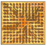
Kilopass’s technology works in a standard process using antifuse, causing a breakdown of the gate-oxide. Since the mechanical damage is so small it is not detectable even by invasive techniques, unlike eFuse technologies where the breaks in the fuse material are clearly visible by inspection. Over the generations of process nodes they have reduced the power by a factor of 10 and reduced the read access time to 20ns. Since the technology scales with the process, the memory can scale as high as 4Mb. It also is low power and instant-on.
Kilopass has focused on 3 major markets:
- security keys and encryption. This only requires Kb of memory. The end markets are set-top box, gaming, SSD, military
- configuration and trimming of analog. This also requires Kb of memory. End markets are power management, high precision analog and MEMS sensors
- microcode and boot code. This requires megabits to tens of megabits. Applications are microcontrollers, baseband and media processors, multi-RF, wireless LAN and more
The diagram above shows how the programming works. There are two transistors per cell. The top one remains a transistor for a 0 (gate isolated from the source/drain) but after programming a 1 the oxide is punched through and the gate has a high resistance short to the drain. Since the actual damage to the gate oxide might occur anywhere (close to the drain or far from it), the resulting resistance is variable.
The traditional way to read the data is as follows. The bitline (WLP) is pre-charged, then the appropriate wordline (WLR) is used for access and the bitline (BL) is sensed and compared against a reference in the sense amp. Depending on whether the “transistor” is a transistor or a resistor, the current will be higher than the reference bitline current or not. If it is higher then a 1 is sensed, lower and a zero. The challenge is to sense the data fast, since the longer the time taken, the clearer the value, but all users want a fast read time. See the diagram below.
Historically this has worked well. In older nodes, the variations are small relative to the drive strengths of the transistors. But increasingly it gets harder to tell the difference between a weak 1 cell and an noisy 0 cell, which risks misreading the value. As a result it can take a long time to sense “to be sure.” As we march down the treadmill of process nodes, like many other things, the variation is getting so large it is approaching the parameters of the device itself. A new approach is needed.
The new approach the Kilopass have pioneered adds a couple of steps. Once the word line is used for access, after a delay the bitline reference is shut off. The bit line is sensed and the data latched and then the sense amp is shut off. The new sense amp incorporates the timing circuitry. The whole scheme is more tolerant of process variation and should be suitable for migration all the way to below 10nm. This approach is more immune to ground noise and has greater discrimination between weak 1 and noisy 0. Finally, shutting off the sense amp at the end saves power.
It turns out that this scheme works particularly well with TSMC’s process since their I[SUB]ref[/SUB] spread is half that of other fabs. The new sensing scheme coupled with tighter cell means doubling the read speed.
Four Takeaways from the TSMC OIP 2015
Paul M. did an excellent job summarizing the technical information that TSMC presented at the recent Open Innovation Platform symposium. I’d like to also share an impression on four areas that struck me as key to TSMC’s strategy.
TSMC OIP: What to Do With 20,000 Wafers Per Day
Today it is TSMC’s OIP Ecosystem Innovation forum. This is an annual event but is also a semi-annual update on TSMC’s processes, investment, volume ramps and more. TSMC have changed the rules for the conference this year: they have published all the presentations by their partners/customers. Tom Quan of TSMC told me that they will also provide a subset of the presentations TSMC gave to open the day.
The semiconductor business is driven by several large markets, the biggest of which is mobile. Fun statistics of the day are that mobile grew 26% from 2014-15 to shipments of 1.9B units. Since there are 4.3B worldwide mobile users, this means that the annual replacement rate is close to 50%. Global mobile traffic is forecast to go up 10X in 5 years from 30EB/yr in 2014 to 292EB/yr in 2019 (EB is exabyte).
For the future, the three big markets other than mobile are Internet of Things (IoT), Automotive, and High-performance Computing (HPC).
Let’s start with IoT: the market has a forecast CAGR from 2013 to 2018 of 21%. But the market is ripe in that 99.4% of devices are notconnected, so by 2022 the average house is forecast to have 500 smart devices. Of course every time you blink the IoT forecast goes up by a billion units but for sure it is real.
The big opportunity in automotive in the medium term is driverless cars or, before that, advanced driver assist systems (ADAS). Google’s driverless cars have done over 2M miles (with 16 minor accidents, all the fault of the other vehicle). Delphi/Audi drove a vehicle across the US from SF to NY (that I wrote about during DAC). Tesla will have autopilot in all their cars. One interesting potential change that autonomous vehicles might bring is to ownership. If you could have a car on-demand whenever you wanted one, would you own your own vehicle at all. Your car plan in a decade might be like your cellphone plan today, with various options depending on usage.
HPC is required to provide the back-end for all those mobile devices, typically in large datacenter aka cloud computing. The need for low latency and location awareness means that the mobile device needs to be providing local intelligence, but then low latency connect to the datacenter will be required too. This means that there will be upgrade cycles to all the base stations, of which there are (literally) millions.
TSMC provides a wide range of processes for different types of silicon. The process nodes mentioned here are where TSMC is working on bringing the process up; volume production is one (or sometimes two) nodes behind.
[TABLE] class=”cms_table_outer_border” style=”width: 240px”
|-
| class=”cms_table_outer_border_td” | Application
| class=”cms_table_outer_border_td” | Technology
|- class=”cms_table_outer_border_tr”
| class=”cms_table_outer_border_td” | MEMS
| class=”cms_table_outer_border_td” | 0.13um
|- class=”cms_table_outer_border_tr”
| class=”cms_table_outer_border_td” | Image Sensor
| class=”cms_table_outer_border_td” | 40nm
|- class=”cms_table_outer_border_tr”
| class=”cms_table_outer_border_td” | Embedded flash
| class=”cms_table_outer_border_td” | 28nm
|- class=”cms_table_outer_border_tr”
| class=”cms_table_outer_border_td” | RF
| class=”cms_table_outer_border_td” | 16nm
|- class=”cms_table_outer_border_tr”
| class=”cms_table_outer_border_td” | Logic
| class=”cms_table_outer_border_td” | 7nm
|- class=”cms_table_outer_border_tr”
| class=”cms_table_outer_border_td” | Analog
| class=”cms_table_outer_border_td” | 16nm
|- class=”cms_table_outer_border_tr”
| class=”cms_table_outer_border_td” | High voltage
| class=”cms_table_outer_border_td” | 40nm
|- class=”cms_table_outer_border_tr”
| class=”cms_table_outer_border_td” | Embedded DRAM
| class=”cms_table_outer_border_td” | 40nm
|- class=”cms_table_outer_border_tr”
| class=”cms_table_outer_border_td” | BCD/power
| class=”cms_table_outer_border_td” | 0.13um
|-
R&D overall is up 19% year-on-year from 2014 to 2015. It was $1.9B in 2014 and will be $2.2B in 2015. OIP has grown and now has over 200 PDKs, 7500 technology files and 8500 IP blocks. The wafers enabled by this IP grew at a CAGR of 22% from 2005-14. Capex is up 10-16% from 2014 to about $10.5B to $11B, compared to $9.5B last year. Total capacity is 1.6M 8″ equivalent wafers per month, over 20,000 per day, up 12% year-on-year.
UPDATE: I totally messed up the title of this blog and the computation. It is over 50,000 wafers per day or over 200 per hour.
New processes are ramping faster than ever. N40 ramped in 35 months. N28 ramped in 22 months. N20 ramped in 3 months. N16 is ramping even faster. At this rate volume production will be faster than qual!
The second presentation was by Jack Sun, TSMC’s CTO. I tried to take notes on the processes but there was too much information. I’ll revisit this once I get some slides to work from. But in the meantime, here are a few highlights.
- N10 will be risk production in Q4 of 2015. Development is on-track.
- N7 will be risk production Q1 of 2017. SRAM test-chip is functional.
- 16FFC will be risk production in Q2 2016
- 16FF+ is in volume production, with a couple of dozen takeouts and 50 more expected before end of year
The key new process coming soon is 16FFC, which is the third generation of 16nm process. Speedup is 65% vs 28nm and 40% vs 20nm. Or a power saving for 70% vs 28nm or 60% vs 20nm. It can go down to 0.55V. TSMC have repeatedly stated that 16FFC will be a long-lived node, which I take to mean that 16FFC will be cheaper per transistor than N28. The design rules are the same so migrating designs and IP should be fairly straightforward. There is a new library coming that will allow operation down to 0.4V, with a focus on minimizing the non-gaussian variation.
N10 has a scale factor of 50% versus 16FF+, with a performance improvement of 20% or a power saving of 40%. There are 3 different Vt and gate-length bias covering a wide range of leakage/speed envelopes. N10 SRAM is yielding well, SERDES runs at 56Gbps with 22% better power efficiency than 16FF+.
N7 has a further speed improvement of 10-50% versus N10, or a power saving of 25-30%. It will be 1.6X the density. Risk production will be Q1 of 2017. Initially libraries for mobile, but new second generation libraries with taller cells for HPC. Special SRAM for HPC too, with 25% better performance. There is an ARM Cortex-A57 test chip showing 40-45% are reduction.
But the roadmap doesn’t end there. TSMC is doing research on Ge FinFET, III-V NFET, gate-all-around nanowires, 2D crystal, directed self-assembly, multi-e-beam direct write, inverse computational lithography. And, of course, EUV. TSMC have achieved 90W source power in-house. ASML have demonstrated 130W. They are working jointly to get all the settings worked out for 125 wafer/hour production.
Other segments. CMOS Image Sensor (CIS):
- FSI front image sensor
- BSI back image sensor (the die is thinned and the light comes through the back)
- BSI/ISP back image sensor flipped onto an image signal processor
- NIR near-infra-red
MEMS
- accelerometer
- pressure sensor
- motion sensor
- microphone
- new gas sensors
- new biometric sensors
Emerging new memories:
- eRRAM
- eMRAM
This is all from my handwritten notes. If you spot errors then correct me in the comments.
SoC and Foundry Update 2H 2015!
Rarely do I fly first class but I did on my recent trip to Asia. It was one of the new planes with pod-like seats that transforms into a bed. The flight left SFO at 1 A.M. so I fell asleep almost immediately missing the first gourmet meal. About half way through the flight I found myself barely awake staring straight up and what do I see? STARS! That has got to be one of the last things anyone wants to see while looking up on an international flight! Seriously, who puts fake stars on the ceiling of an airplane! EVA Airlines that’s who!
When I travel a lot of people want to meet with me to get the latest news from Silicon Valley. In exchange I get the latest news from wherever they are so it is a very nice quid pro quo type of thing, absolutely. The most common topics are the SoC and foundry business since they currently drive the semiconductor industry. Apple and Qualcomm are the most talked about SoC companies but Mediatek, Samsung, and even Intel are always discussed.
Let’s start with Apple: The big iProduct announcement is next week and we will finally get to see what is inside the iPhone 6s! Again, my bet is a Samsung based 14nm A9 SoC and inside the new iPads will be a TSMC based 16nm A9x SoC. I was right on the iPhone 5s (Samsung 28nm) and iPhone 6 (TSMC 20nm) so let’s see if I can keep my streak going. My bet is also that the Apple A9x will outperform all other SoCs and will continue to do so until mid to late next year.
Moving forward it is my bet that Apple will continue with TSMC 16nm for the iPhone7 with an enhanced version of the process specifically for Apple. Based on what I know today 10nm will not be in production in time for the iPhone 7 but could make it for the next iPads since iPads come out later in the year and require less volume. Currently Samsung and TSMC both have pre-production 10nm PDKs available but final decisions by the fabless elite have not been made. We should know more about where the fabless elite will fab 10nm at the end of this year. I would not expect 10nm production to start before Q2 2017 as there have been delays. The iProduct refresh in 2017 however will be 10nm for sure.
QCOM has a history of 2[SUP]nd[/SUP], 3[SUP]rd[/SUP], and even 4[SUP]th[/SUP] sourcing chip manufacturing down to 40nm. At 28nm everyone was forced into a monogamous relationship with TSMC which was very uncomfortable for a promiscuous company like QCOM. At 28nm QCOM is now in production at UMC and hopes to get ramped up at SMIC to appease the Chinese gods. QCOM as we have all heard will use both Samsung 14nm and GlobalFoundries 14nm for the next generation of Snapdragons. I’m also told that QCOM will use TSMC 16FF+ and they have a 14nm development agreement with SMIC in process.
Mediatek of course manufactures next door (literally) at TSMC and UMC and I do not see that changing anytime soon. Mediatek has hit semiconductor rock star status in Taiwan and they have attracted many ex TSMC and UMC employees. Not only does this give Mediatek leading edge design experience, it also gives them access to the inner foundry ranks. Given the importance of low power design for mobile I would bet Mediatek products will be FinFET enabled next year with the rest of the fabless elite so watch out QCOM!
I’m sorry, I ran out of space for more commentary. If you have questions we can continue the discussion in the comments section. Only registered SemiWiki members can read or write comments so if you are not already a SemiWiki member please join as my guest: https://www.legacy.semiwiki.com/forum/register.php