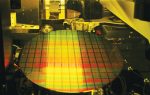
TSMC, the largest and most influential pure-play foundry, has many fascinating stories to tell. In this section, TSMC covers some of their basic history, and explains how creating an ecosystem of partners has been key to their success, and to the growth of the semiconductor industry.
The history of TSMC and its Open Innovation Platform (OIP)® is, like almost everything in semiconductors, driven by the economics of semiconductor manufacturing. Of course, ICs started 50 years ago at Fairchild (very close to where Google is headquartered today, these things go in circles). The planarization approach, whereby a wafer (just 1” originally) went through each process step as a whole, led to mass production. Other companies such as Intel, National, Texas Instruments and AMD soon followed and started the era of the Integrated Device Manufacturer (although we didn’t call them that back then, we just called them semiconductor companies).
The next step was the invention of ASICs with LSI Logic and VLSI Technology as the pioneers. This was the first step of separating design from manufacturing. Although the physical design was still done by the semiconductor company, the concept was executed by the system company. Perhaps the most important aspect of this change was not that part of the design was done at the system company, but rather the idea for the design and the responsibility for using it to build a successful business rested with the system company, whereas IDMs still had the “if we build it they will come” approach, with a catalog of standard parts.
In 1987, TSMC was founded and the separation between manufacture and design was complete. One missing piece of the puzzle was good physical design tools and Cadence was created in 1988 from the merger of SDA and ECAD (and soon after, Tangent). Cadence was the only supplier of design tools for physical place and route at the time. It was now possible for a system company to buy design tools, design their own chip and have TSMC manufacture it. The system company was completely responsible for the concept, the design, and selling the end-product (either the chip itself or a system containing it). TSMC was completely responsible for the manufacturing (usually including test, packaging and logistics too).
At the time, the interface between the foundry and the design group was fairly simple. The foundry would produce design rules and SPICE parameters for the designers; the design would be given back to the foundry as a GDSII file and a test program. Basic standard cells were required, and these were available on the open market from companies like Artisan, or some groups would design their own. Eventually TSMC would supply standard cells, either designed in-house or from Artisan or other library vendors (bearing an underlining royalty model transparent to end users). However, as manufacturing complexity grew, the gap between manufacturing and design grew too. This caused a big problem for TSMC: there was a lag from when TSMC wanted to get designs into high volume manufacturing and when the design groups were ready to tape out. Since a huge part of the cost of a fab is depreciation on the building and the equipment, which is largely fixed, this was a problem that needed to be addressed.
At 65 nm TSMC started the Open Innovation Platform (OIP) program. It began at a relatively small scale but from 65 nm to 40 nm to 28 nm the amount of manpower involved went up by a factor of 7. By 16 nm FinFET, half of the design effort is IP qualification and physical design because IP is used so extensively in modern SoCs, OIP actively collaborated with EDA and IP vendors early in the life-cycle of each
process to ensure that design flows and critical IP were ready early. In this way, designs would tape-out just in time as the fab was starting to ramp, so that the demand for wafers was well-matched with the supply.
In some ways the industry has gone a full circle, with the foundry and the design ecosystem together operating as a virtual IDM. The existence of TSMC’s OIP program further sped up disaggregation of the semiconductor supply chain. Partly, this was enabled by the existence of a healthy EDA industry and an increasingly healthy IP industry. As chip designs had grown more complex and entered the SoC era, the amount of IP on each chip was beyond the capability or the desire of each design group to create. But, especially in a new process, EDA and IP qualification was a problem.
On the EDA side, each new process came with some new discontinuous requirements that required more than just expanding the capacity and speed of the tools to keep up with increasing design size. Strained silicon, high-K metal gate, double patterning and FinFETs each require new support in the tools and designs to drive the development and test of the innovative technology.
On the IP side, design groups increasingly wanted to focus all their efforts on parts of their chip that differentiated them from their competition, and not on re-designing standard interfaces. But that meant that IP companies needed to create the standard interfaces and have them validated in silicon much earlier than before.
The result of OIP has been to create an ecosystem of EDA and IP companies, along with TSMC’s manufacturing, to speed up innovation everywhere. Because EDA and IP groups need to start work before everything about the process is ready and stable, the OIP ecosystem requires a high level of cooperation and trust.
When TSMC was founded in 1987, it really created two industries. The first, obviously, is the foundry industry that TSMC pioneered before others entered. The second was the fabless semiconductor companies that do not need to invest in fabs. This has been so successful that two of the top 10 semiconductor companies, Qualcomm and Broadcom, are fabless and all the top FPGA companies are fabless.
The foundry/fabless model largely replaced IDMs and ASIC. An ecosystem of co-operating specialist companies innovates fast. The old model of having process, design tools and IP all integrated under one roof has largely disappeared, along with the “not invented here” syndrome that slowed progress since ideas from outside the IDMs had a tough time penetrating. Even some of the earliest IDMs from the “Real men have fabs” era have gone “fab lite” and use foundries for some of their capacity, typically at the most advanced nodes.
Legendary TSMC Chairman Morris Chang’s “Grand Alliance” is a business model innovation of which OIP is an important part, gathering all the significant players together to support customers—not just EDA and IP, but also equipment and materials suppliers, especially for high-end lithography.
Digging down another level into OIP, there are several important components that allow TSMC to coordinate the design ecosystem for their customers.
- EDA: the commercial design tool business flourished when designs got too large for hand-crafted approaches and most semiconductor companies realized they did not have the expertise or resources in-house to develop all their own tools. This was driven more strongly in the front-end with the invention of ASIC, especially gate-arrays; and then in the back end with the invention of
- IP: this used to be a niche business with a mixed reputation, but now is very important with companies like ARM, Imagination, CEVA, Cadence, and Synopsys, all carrying portfolios of important IP such as microprocessors, DDRx, Ethernet, flash memory and so on. In fact, large SoCs now contain over 50% and sometimes as much as 80% TSMC has well over 5,500 qualified IP blocks for customers.
- Services: design services and other value-chain services calibrated with TSMC process technology helps customers maximize efficiency and profit, getting designs into high volume production rapidly
- Investment: TSMC and its customers invest over $12 billion a year. TSMC and its OIP partners alone invest over $1.5 billion. On advanced lithography, TSMC has further invested $1.3 billion in
Processes are continuing to get more advanced and complex, and the size of a fab that is economical also continues to increase. This means that collaboration needs to increase as the only way to both keep costs in check and ensure that all the pieces required for a successful design are ready just when they are needed.
TSMC has been building an increasingly rich ecosystem for over 25 years and feedback from partners is that they see benefits sooner and more consistently than when dealing with other foundries. Success comes from integrating usage, business models, technology and the OIP ecosystem so that everyone succeeds. There are a lot of moving parts that all have to be ready. It is not possible to design a modern SoC without design tools, more and more SoCs involve more and more 3rd party IP, and, at the heart of it all, the process and the manufacturing ramp with its associated yield learning all needs to be in place at TSMC.
The proof is in the numbers. Fabless growth in 2013 is forecasted to be 9%, over twice the increase in the overall industry at 4%. Fabless has doubled in size as a percentage of the semiconductor market from 8% to 16% during a period when the growth in the overall semiconductor market has been unimpressive. TSMC’s contribution to semiconductor revenue grew from 10% to 17% over the same period.
The OIP ecosystem has been a key pillar in enabling this sea change in the semiconductor industry.
TSMC 2019 Update
2019 TSMC Technology Symposium Review Part I
TSMC Technology Symposium Review Part II
Global Unichip Corporation
Another facet of TSMC is GUC, Global Unichip Corporation. It is a partially owned subsidiary and also an important partner, providing design services and allowing TSMC themselves to continue to be a pure-play foundry. GUC was founded in 1998 with 10 employees as what has come to be known as a “Design Service” company. It ramped fast and by 2000 it employed over 100 people.
The years between 2003 and 2010 were milestone years for GUC, representing a period of unprecedented growth. The era was marked by a strengthening of both business and technology relationships with the largest semiconductor foundry in the world, TSMC. That relationship set GUC on firm growth, bringing over the core of today’s management and the business strategy that guides the company today.
In 2003, TSMC assumed an ownership stake in GUC. But the foundry leader’s investment went far beyond financial investment. Part of its strategy to enhance the return on its investment was to move GUC to a global business strategy and put it on the road to being an advanced technology leader.
The technology model, and the business model that accompanied it, soon began to gain traction. Prior to 2003, much of GUC’s business came from the consumer electronics companies who tended to utilize more mature technologies and were primarily located in Taiwan. With the installation of new management, and new business and technology models, business emphasis began to migrate to the more technically sophisticated networking and communications sectors that required more advanced technologies. In 2004, 100% of GUC’s revenue was at the 0.13 µm technology node; by 2005, 5% of revenue came from the new 90 nm node and a year later, an additional 3% of revenue came from the emerging 65 nm node.
The impact of this trend was soon seen in the company finances. Revenue jumped from $20 million in 2002 to $27 million in 2003, $32 million in 2004, and a whopping $48 million in 2005—more than doubling the revenue over a four year period.
The year 2006 marked another major milestone. In the third quarter of that year, GUC became a publicly traded company when it offered its shares on the Taiwan Stock Exchange.
The operations side instituted a major focus on advanced technology. In 2007, the company developed an advanced technology digital design flow, followed shortly thereafter by a low power design flow. As a result, the company saw a large increase in the size of their designs, many with gate counts jumping exponentially. In the face of an industry-wide recession in 2009, GUC showed its confidence in the future by investing heavily in internal IP development, in particular, IP targeting the networking market segment.
This era of prosperity was reflected by a broad set of indices. Annual revenue in 2006 more than doubled that of 2005 ($48 million) at $103 million, then more than doubled again in 2007 to $216 million. In 2008, revenue jumped to $295 million before falling during the recession of 2009 to $252 million. In 2008, GUC saw a jump in revenue from advanced technology to 21 % and to 34 % in 2009, with 1 % of that coming from leading edge 40 nm products. Like all technology companies, GUC experienced a financial decline in 2009, with revenues dropping to $252 million.
But the company would rebound quickly in 2010, posting revenues of $327 million with advanced technologies accounting for 42% of that total. The year also proved auspicious. Driven by the recession to examine its business model, GUC would begin making a series of strategic decisions that would allow it to capitalize on a new era of semiconductor device design.
The company’s growth as an innovative force in the semiconductor industry is also reflected in the number of new employees required to implement increasingly complex technologies. At the end of 2003, GUC employed 132 people, most of them in Taiwan. Three years later, that number had more than doubled to 287 and by the start of 2010, the company counted 484 employees, a number that has held relatively steady through 2013. Employee growth was fueled by expanded geographic growth. GUC opened its first international office when it established a subsidiary in North America (GUC N.A.) in February of 2004 and then opened its Japan office in June of 2005. Nearly three years later, in May of 2008, the company opened its third international office, GUC Europe, in Amsterdam, The Netherlands and one month later opened an office in Korea. GUC entered the fast-growing China market when it opened an office in one of that country’s technology hubs near Shanghai in 2009.
Success in the semiconductor industry going forward is going to be heavily weighted by the ability to leverage industry’s third-party infrastructure that has now matured. Foundries are at the leading edge of the infrastructure, providing the most advanced process technologies, as well as specialized technologies to all comers. IP and chip design implementation are also being outsourced, cost-effectively utilizing technology and financial resources.
It is in this new and exciting environment that GUC evolved the Flexible ASIC Model, which is designed to provide the most effective, efficient and flexible path to semiconductor innovation.
The Flexible ASIC Model is a response to both the business and technical challenges facing today’s semiconductor companies. This model allows companies to allocate their resources more efficiently. It brings together design expertise, systems knowledge and manufacturing resources to efficiently drive delivery of the final packaged IC. The model’s basic strategy is to spread design risks and to minimize IDM, fabless and OEM (Original Equipment Manufacturers) upfront semiconductor-related fiscal and human capital investments. The goal is to increase the efficiency of the entire value chain, from concept to delivery; to shorten all phases of the development cycle; and to ultimately increase device yield quality and reliability.
At the heart of the Flexible ASIC Model is integrated manufacturing. GUC has made a strategic choice to work exclusively with TSMC, the semiconductor industry’s leading foundry service company. It is this relationship that plays an integral role in the company’s ability to achieve early advanced technology access and match designs to manufacturing resources.
Spotlight: Dr. Morris Chang
Dell changed the way personal computers are manufactured and sold. Starbucks changed the amount we would pay for a cup of coffee. eBay took the yard sale out of our yards. TSMC took the semiconductor manufacturing costs off our balance sheets and out of our capital investments.
It’s hard to overstate the impact that Dr. Morris Chang, Founder, Chairman, and until-recently CEO of TSMC, has had on the industry. He has been influential as a leader in business model innovation, and has earned his company roughly 50% of the foundry market share.
Chang left his native China in 1949, moving to the US to attend Harvard University. He soon transferred to MIT as he followed his interest in technology. After earning his MS in 1953 from MIT’s mechanical engineering graduate school, Morris went directly into the semiconductor industry at the process level with Sylvania Semiconductor and was quickly moved to management.
Chang moved to Texas Instruments in 1958, where he stayed for 25 years, rising to VP of the worldwide semiconductor business (and also earned a PhD in electrical engineering from Stanford in 1964). At TI, he worked on a four transistor project in which the manufacturing was done by IBM, thus engaging in one of the early semiconductor-foundry relationships. Also at TI, Chang developed a new model of semiconductor pricing that sacrificed early profits to gain market share and to achieve manufacturing yields that would lead to higher long-term profits.
Chang left TI in 1983 and did a short stint at General Instrument Corporation. He then moved to Taiwan to head the Industrial Technology Research Institute (ITRI), which led to the founding of TSMC.
Chang noticed in the early 1980s, while at TI and GI, that top engineers were leaving and forming their own semiconductor companies. Unfortunately, the heavy capital requirement of semiconductor manufacturing was a gating factor. The cost back then was $5-10 million to start a semiconductor company without manufacturing and $50-100 million to start a semiconductor company with manufacturing. Some of these start-ups used excess capacity from IDMs but were subjected to uncertainties in foundry capacity and sometimes had to buy wafers from a competitor. Around this time, 1985, the first truly fabless startups, like Xilinx and Chips and Technologies, were launched and doing well.
It was in 1987, within this nascent fabless environment, that Chang started TSMC. Although TSMC started two process nodes behind where semiconductor manufacturers (IDMs) were at the time, they had the advantage of being a pure-play foundry, not a competitor. Their focus was on their customers.
Morris Chang made the first TSMC sales calls with a single brochure: TSMC Core Values: Integrity, Commitment, Innovation, Partnership. Four or five years later, TSMC was only behind by one process node and the orders started pouring in. In 10 years, TSMC caught up with IDMs (except for Intel) and the fabless semiconductor industry blossomed, enabling a whole new era of semiconductor design and manufacturing. In the last 20 years, and still today, even the remaining IDMs are being forced to go fabless or fab-lite at 28 nm and below due to high costs and daunting technical challenges.
Dr. Morris Chang in 2007.
Dr. Morris Chang turned 82 on July 10th, 2013. He is still running TSMC full time as the founding Chairman. He works from 8:30 am to 6:30 pm like most TSMC employees and says that a successful company life cycle is: rapid expansion, a period of consolidation, and maturity. The same could be said about Chang himself.
2019 Update: Dr. Morris Chang
In 2017 the TSMC Museum of Innovation opened Under Fab 12 in Hsinchu Taiwan. It not only commemorates the history of semiconductors and TSMC but also the life of Dr. Morris Chang. Morris Chang’s wife Sophie was actively involved in this project:
The TSMC Museum of Innovation encompasses three exhibition galleries: “A World of Innovation,” “Unleashing Innovation,” and “Dr. Morris Chang, TSMC Founder.” Through interactive technology, digital content, and historical documents we will learn about the pervasiveness of ICs in our daily lives and about their continued advancement. In addition, we will learn how ICs are making our lives more fulfilling and how they are driving technology beyond our imagination. We will also learn how TSMC contributes to global IC innovation and to Taiwan’s economy.
In 2018 Dr. Morris Chang retired from TSMC for the second and final time:
TSMC Dr. Morris Chang Announces Retirement in June 2018. Future Dual Leadership Will Be Mark Liu as Chairman And C.C. Wei as CEO.
Issued by: TSMC Issued on: 2017/10/02
Hsinchu, Taiwan, R.O.C. – Oct. 2, 2017 – TSMC Chairman Morris Chang today announces: “I will retire from the Company immediately after the Annual Shareholders Meeting in early June, 2018. I will not be a director in the next term of the board of directors. Nor will I participate in any TSMC management activities after the Annual Shareholders Meeting in early June, 2018. From early June, 2018 on, TSMC will be under the dual leadership of Dr. Mark Liu and Dr. C.C. Wei. Dr. Mark Liu will be the Chairman of the Board, and Dr. C.C. Wei will be the Chief Executive Officer. All present directors of the board have agreed to be nominated, and if elected, serve as directors of the board during the next term. They have also agreed to support the aforementioned dual leadership of the Company under Drs. Liu and Wei. Chairman Morris Chang further said, “The past 30-odd years, during which I founded and devoted myself to TSMC, have been an extraordinarily exciting and happy phase of my life. Now, I want to reserve my remaining years for myself and my family. Mark and CC have been Co-CEO’s of the Company since 2013 and have performed outstandingly. After my retirement, with the continued supervision and support of an essentially unchanged board, and under the dual leadership of Mark and CC, I am confident that TSMC will continue to perform exceptionally.”