Technological leadership has long been key to TSMC’s success and they are following up their leadership development of 5nm with the world’s smallest SRAM cell at 0.021um 2 with circuit design details of their write assist techniques necessary to achieve the full potential of this revolutionary technology. In addition to their groundbreaking device developments such as High Mobility Channel (HMC) they are the leading implementers of Extreme Ultra-Violet (EUV) patterning to enable higher yield and shorter cycle time at this advanced node.
Semiconductor technology evolution has been driven by the application landscape which in the current phase of High-Performance Computing (HPC), Artificial Intelligence (AI) and 5G communication requires the highest performance with limited power dissipation as illustrated in Fig. 1.
Fig. 1 Semiconductor Technology Application Evolution
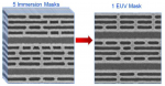
This technology was described by TSMC at IEDM 2019, where they described their 5 nm process which uses more than 10 Extreme Ultra-Violet (EUV) mask patterning steps replacing three or more immersion mask steps each and High Mobility Channel (HMC) technology for higher performance. This technology has been in risk production since April of 2019 and will be in full production 1H2020.
The implementation of this technology for the development of high- performance SRAM bit cells and arrays was described by Jonathan Chang, et al at ISSCC2020.
The quantizing of FinFET transistor sizing continues to be a major challenge and forces all transistors in the high-density 6T SRAM cell to use only a single fin. The design is optimized through Design-Technology Co- Optimization (DTCO) to give high performance and density as well as high yield and reliability. SRAM bit cell scaling for 2011 to 2019 is shown in Fig. 2.
Fig. 2. SRAM bit cell scaling is shown for 2011 to 2019.
It can be noted that the cell size reduction rate from 2017 to 2018 to 2019 is much slower than the rate for preceding years 2011 to 2017, showing that SRAM cells have not been scaling at the same rate as logic in general. At IEDM 2019, the 5nm process was quoted to have 1.84x logic density improvement compared to 1.35x SRAM density improvement. Further area reduction utilizing Flying Bit Line (FBL) architecture is implemented for 5% area savings. The layout of the 5nm cell is shown in Fig. 3.
Fig. 3. Layout of the high-density 6T SRAM bit cell.
For power reduction, a key approach is lowering the minimum operating voltage Vmin of the SRAM array. The increased random threshold voltage variation in this latest technology limits Vmin which in turn limits the opportunities for power reduction. The SRAM voltage scaling trend is shown in Fig. 4, where the blue line indicates the Vmin without write assist and the red line indicates Vmin with write assist, showing great benefit of write assist with each generation. It will be observed that the Vmin from 7nm to 5nm shows very little improvement, indicating that further power reduction must be gotten from improvements in write assist generation circuits. This article will describe the major write assist methods to enable lower Vmin in operation, negative bit line (NBL) and Lower Cell VDD (LCV).
Fig. 4. SRAM cell voltage scaling trend without write assist (blue line) and
with write assist (red line).
The SRAM cell schematic is shown in Fig. 5 showing contention during write between the PU and pass-gate transistor PG. A stronger PU transistor would yield a higher read stability, but it degrades the write margin significantly and results in a contention write Vmin issue.
Fig. 5. SRAM cell schematic showing contention during write between the
PU and pass-gate transistor PG.
The first method to improve the write Vmin is to lower the bit line voltage during write, called Negative Bit Line or (NBL). This method has been employed for several years, using a MOS capacitor to generate a negative bias signal on the bit line, but this write assist circuitry results in area overhead. Furthermore, a fixed amount of MOS capacitance induces over boosted NBL level for short BL configuration and may led to dynamic power overhead in short bit lines, as shown in Fig. 6.
Fig. 6. Fixed amount of MOS capacitance induces over-boosted NBL level
for short BL configuration and may lead to dynamic power overhead
avoided by the metal cap NBL.
The overboost and the MOS capacitor area issues can be avoided by using a metal capacitor-coupled scheme based on coupled metal tracks laid out on top of the upper metal of the SRAM array. To avoid the overboost, the metal capacitor length can be modulated with the SRAM array bit line length, saving dynamic power. Furthermore, the coupled NBL level can also be adjusted to compensate the loss of write ability induced by BL IR drop on the far-side bit cell.
The NBL enable signal (NBLEN) in Fig. 7 drives one side of the metal capacitor C1 negative which couples a negative bias signal at the virtual
ground node NVSS which then passes through the write driver WD and column multiplex to the selected bit line.
Fig. 7. The NBL enable signal (NBLEN) couples the configurable metal
capacitor C1 to NVSS.
The NBL coupling level with different bit line configurations, Fig. 8, showing that the configurable metal capacitor C1 can track with bit line length so that the variation of the coupling NBL level with different Bit line length can be mitigated.
Fig. 8. NBL coupling level with different bit line configurations showing the
longer 256bit bitline (blue) having an extended NBL boosted level.
The second method of write assist is to Lower the Cell VDD, (LCV). The conventional techniques of LCV require a strong bias or an active-divider to adjust the column-wise bit cell power supply during write operation, but these techniques consume a huge amount of active power across operating time. Pulse Pull-down (PP) and Charge Sharing (CS) techniques are two alternative solutions but precise timing is difficult for PP, so CS is proposed using metal wire charge sharing capacitors on top of the array as shown in Fig. 9.
Fig. 9. Charge Sharing (CS) for Low Cell VDD (LCV) for write assist using
CS metal tracks on top of the SRAM array.
In write operation, the LCV enable signal (LCVEN) goes high, it turns off the pull low NMOS (N1) to isolate the charge sharing capacitor C1 from ground. A column is selected by COL[n:0] to turn the header P0 off and isolates the array virtual power rail CVDD[0] from true power VDDAI. Because the metal wire capacitance scales along with the size of the bit-cell array, it also benefits the SRAM compiler design and provides a relatively constant charge sharing voltage level with varied BL configurations. The charge sharing level is determined by metal capacitance ratio of CVDD and the charge sharing metal track. Fig. 10 shows three LCV-VDD ratios are implemented for 6%, 12% and 24%.
Fig. 10. Three LCV-VDD ratios are implemented for 6%, 12% and 24%.
With write assist turned off, Vmin is constrained by write failure. Measured
results with Write Assist in Fig. 11 show NBL improves Vmin by 300mV and 24% LCV improves Vmin independently by over 300mV.
Fig. 11. Measured results of (a) metal capacitor-boosted Write Assist
WAS-NBL scheme and (b) metal charge-sharing capacitor WAS-LCV
scheme.
Performance of the 5nm process is enhanced by the High Mobility Channel with ~18% drive current gain shown in Fig. 12. This technology was described in detail at IEDM2019.
Fig. 12. High Mobility Channel (HMC) performance gain of ~18%.
This performance gain is exemplified by the high-speed SRAM array for
L1 cache application achieving 4.1Ghz cycle time t 0.85V shown in the
shmoo plot in Fig. 13.
Fig. 13. Shmoo plot of the HD SRAM array for use as a high performance
L1 cache showing 4.1 GHz at 0.85V. The measured results are based on the 135 Mb test chip shown in Fig. 14.
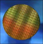
Fig. 14. 135 Mb test chip in 5 nm HK-MK FinFET with High Mobility
Channel (HMC) and 0.021um 2 SRAM bit cell.
In summary, the detailed circuit design techniques described here enable the product developer to get the maximum advantage from this leading technology. An important device development approach is to do Design- Technology Co-optimization (DTCO) between product/circuit designers and process developers responsible for product yield and reliability.