– The new M1 chip unveils previously hidden asset
– Could/should Apple sell semiconductors?
– Are servers next?
– The M1 chip appears to be a rousing success and the beginning of a new era
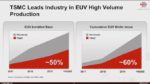
Essentially 100% of all early reports on the performance of the M1 chip have come back with stellar reviews. Great performance across the board across a multitude of applications while barely sipping power. It checks all the boxes of speed, power , memory, graphics, neural engine etc; Of course this is all enabled by TSMC’s 5NM process which squeezes 16 billion transistors into the M1.
The question from an investors point of view is what this does to the competition as well as what does it do for Apple. The impact cannot be underestimated and could easily extend well beyond what investors currently think and expect.
What would a stand alone “Apple Semiconductor” be worth?
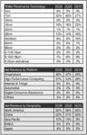
“Apple Semiconductor”, Intel, AMD & Nvidia etc; all seem a lot alike as they are essentially all “fabless” design houses (or will be soon in the case of Intel) that outsource manufacture to TSMC. Nvidia leads with a market cap of $325B, Intel is at $190B and AMD is $103B. Qualcomm is $163B and Broadcom is $157B. Nvidia could get even larger with an ARM acquisition.
Apple didn’t just get into the semiconductor business recently. It’s has been in the business for many years, well over 13 years. Going back to the first iPhone introduced in 2007. Apple’s history and line of of semiconductors would easily rival any current chip maker out there.
Apple’s Chip History
Apple’s breath and depth in semiconductor design and manufacture put it firmly in the big leagues next to any of the top chip makers today. We could easily argue that “Apple Semiconductor” would be worth more than either Intel or AMD. Both Intel and AMD’s primary line of business is making X86 compatible processors for PCs and servers.
The X86 architecture goes way, way back to the original 8086 which was released an astounding 41+ years ago back in 1979. Backward X86 compatibility of todays processors made by Intel and AMD is a blessing and a curse at the same time. It brings a wealth of software that will run on anything X86 compatible but can also act as a drag on overall performance based on a 40+ year old architecture compatibility.
Chip design engineers at both AMD and Intel have never been able to erase the entire blackboard and literally “start with a clean slate”. Apple obviously does not have quite as much history to lug around and in fact just started with a relatively clean slate for the M1 design even while maintaining IOS compatibility.
Back to the days of “Big Hair”
X86 was built in the days of desktop PCs that morphed into laptops and servers even though saddled with power hungry CPUs that were always plugged into a wall socket.
The M1 is designed in the era of smart phones and cloud computing. AI & ML. Stunning graphics and a purpose built parallel architecture. In summary we think that Apple Semiconductor would be worth more than either Intel or AMD.
When we compare Apple Semiconductor to Nvidia and Qualcomm, Broadcom. Apple clearly has much of the capability of Qualcomm, Broadcom in communications and other support semiconductors but perhaps more importantly has one foot, perhaps both feet firmly planted in the future of computers and semiconductors as Nvidia does with AI & graphics capabilities.
Today we can say without exaggeration that Apple makes both the best smart phone chip as well as the best laptop/desktop chip versus anyone.
All this implies that “Apple Semiconductor” as a standalone company would likely surpass the market cap of any and all chip companies currently out there.
This is all well and fine you may say but its merely an academic exercise as “Apple Semiconductor” is inside Apple never to be let out of its “gilded cage” But what if it were free?
Could/Should Apple Attack the Server Market?
Apple’s recent M1 roll out never mentioned the word server. However we think the M1 begs the question as to whether it would and could be dominant in the highly sought after and cash cow market that is the server/cloud market.
Its Intel’s sacred cow and obviously already in AMD’s crosshairs but could Apple swoop in and clean up?
We don’t think that Apple really wants to crank out servers but it could do very well selling CPUs to all the server makers such as Intel does. Heck, Apple could start conversion on their own huge server farm. Maybe sell processors to Google, Amazon and Facebook etc; or all the huge Chinese server farms.
Power & cooling are perhaps the biggest deals in the server world and so far the one of the biggest selling points of the M1 is its low power, fans never go on, design.
The power savings alone could be the reason to switch
We think the idea is not so far fetched as the server / cloud business is an attractive target that Apple has yet to tap and now they clearly have the ammunition to do so.
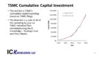
Of course both Intel and AMD will improve once they start producing parts on TSMC’s 5NM or 3NM and beyond but right now Apple has a pretty big lead over both and is TSMC’s biggest customer which gets them an advantage.
From a strategic game, this could even foil Nvidia’s plan for ARM and data center conquest, thus placing Apple Semiconductor well above even Nvidia.
Why stop at server chips?
Of course we can follow the logic of entering the server market with moving into the AI or other markets such as automotive etc; The list and opportunities are long. We do doubt that Apple would ever sell its crown jewel chip technology to competitors but you never know.
Does “Apple Semiconductor” add to $2T market cap?
Its hard to move the needle on a company that’s already pushing a $2T market cap, even a few hundred billion or so.
While its hard to do some additive math here, we think more importantly that it just further underscores Apple’s value and perhaps previously hidden value while also exposing some potential vulnerabilities of existing competitors in the semiconductor business.
Apple is still somewhat limited to being a customer of TSMC but its a very symbiotic relationship much like the “Wintel”, Microsoft/Intel relationship which dominated tech for so long “Apple/TSM Semiconductor Inc” is obviously very formidable and much more so than Wintel ever was.
The stocks
Even though Intel has been very beat up we still remain concerned about how they get out of the current predicament and differentiate from AMD. AMD stock has done well at Intel’s expense but is stuck in a similar technology / market trap that has good short term dynamics but less so longer term.
We think Apple’s move to its own processors will be much faster than expected . Why in the world would I buy a dead end architecture? This could help margins even more. A faster move obviously benefits them.
Levering semiconductors further is currently just a dream but a pretty good one that could easily be executed and makes sense especially in Apple’s quest for growth as its a market that could move the needle even for them.
Sometimes its better to be lucky than smart. Apple’s timing couldn’t be much better given COVID-19, work/school remotely and Intel falling on its own sword. The M1 chip introduction is likely to be a huge success. I’ve been waiting to buy one and now I’m convinced.
Also Read:
2021 will be the year of DRAM!
Post Election Fallout-Let the Chips Fall / Rise Where They May