The most viewed blogs I write for SemiWiki are consistently blogs comparing the four leading edge logic producers, GLOBALFOUNDRIES (GF), Intel, Samsung (SS) and TSMC. Since the last time I compared the leading edge new data has become available and several new processes have been introduced. In this blog I will update the current status.
Leading Edge Processes
Although this data set goes back to 2001 in some cases ,the focus is more current processes. Specifically:
- GF – 14nm and 7nm – full datasets are available, and we have forecast a 5nm process. A 12nm and 7+nm process have been announced and we have forecast them as well.
- Intel – 14nm and 10nm – full datasets are available, and we have forecast 7nm.
- Samsung – 14nm, 10nm and 7nm datasets are available. Samsung has also announced 11nm, 8nm, 6nm, 5nm and 4nm processes and we have forecast them.
- TSMC – 16nm, 10nm and 7nm datasets are available. TSMC has also announced 12nm, 7+nm, 5nm and 3nm processes and we have forecast them.
Standard Cells
Logic designs are built up from standard cells. The height of a standard cell is the metal 2 pitch (M2P) multiplied by the tracks. In the past we have talked about minimum metal pitch (MMP) and tracks, but the tracks are measured in metal 2 and the pitch should be also.
The width of a cell is related to the contacted poly pitch (CPP) with the cell width some number of CPPs depending on the cell type and whether a double diffusion break or single diffusion break is used (more on this later).
Slide 2 illustrates standard cell sizing.
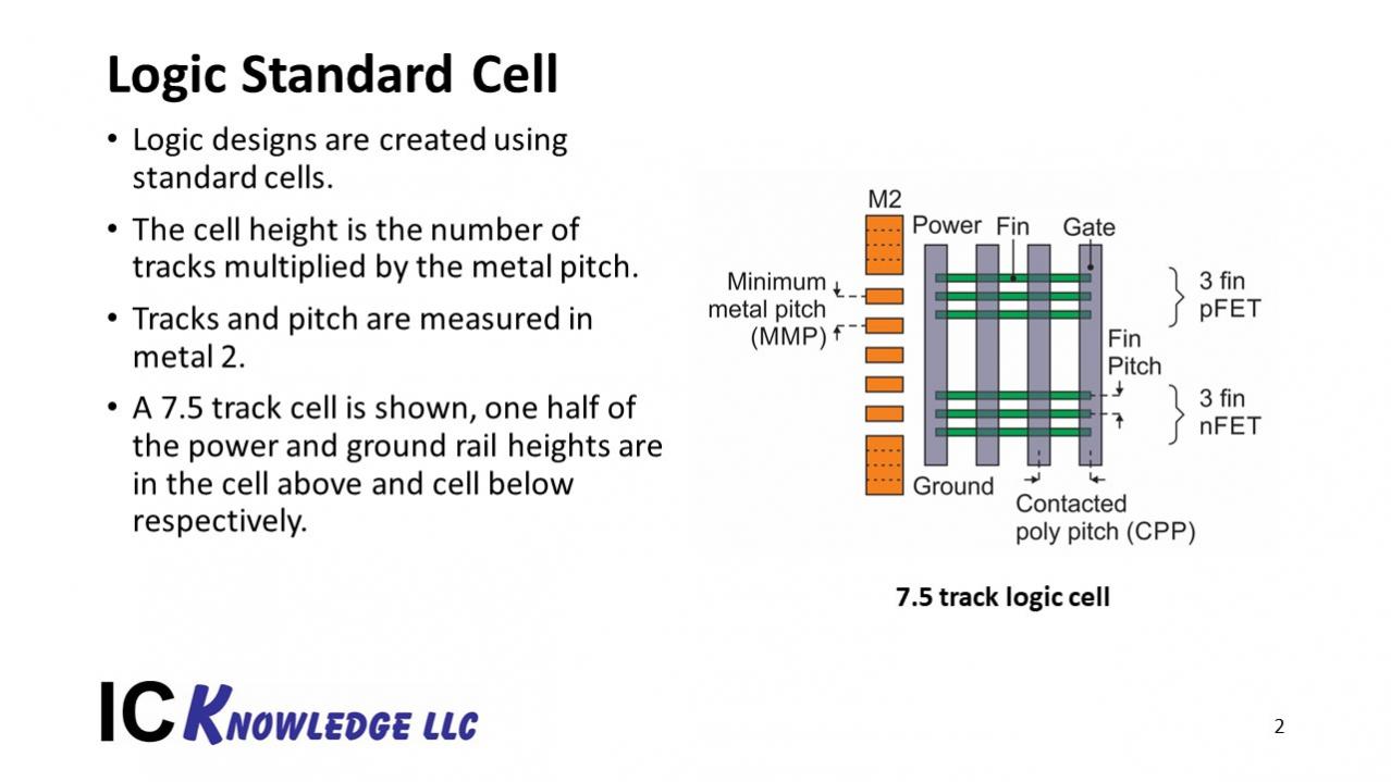
Slide 2. Logic Standard Cell.
Metal 2 Pitch (M2P)
The first metric we need to visit to start comparing logic processes is M2P. The four companies driving the leading edge are GF, Intel, SS and TSMC. In Slide 3 we have plotted M2P versus time for these companies. The solid filled markers are actual known pitches and the unfilled markers are our estimates based on announced density improvements.
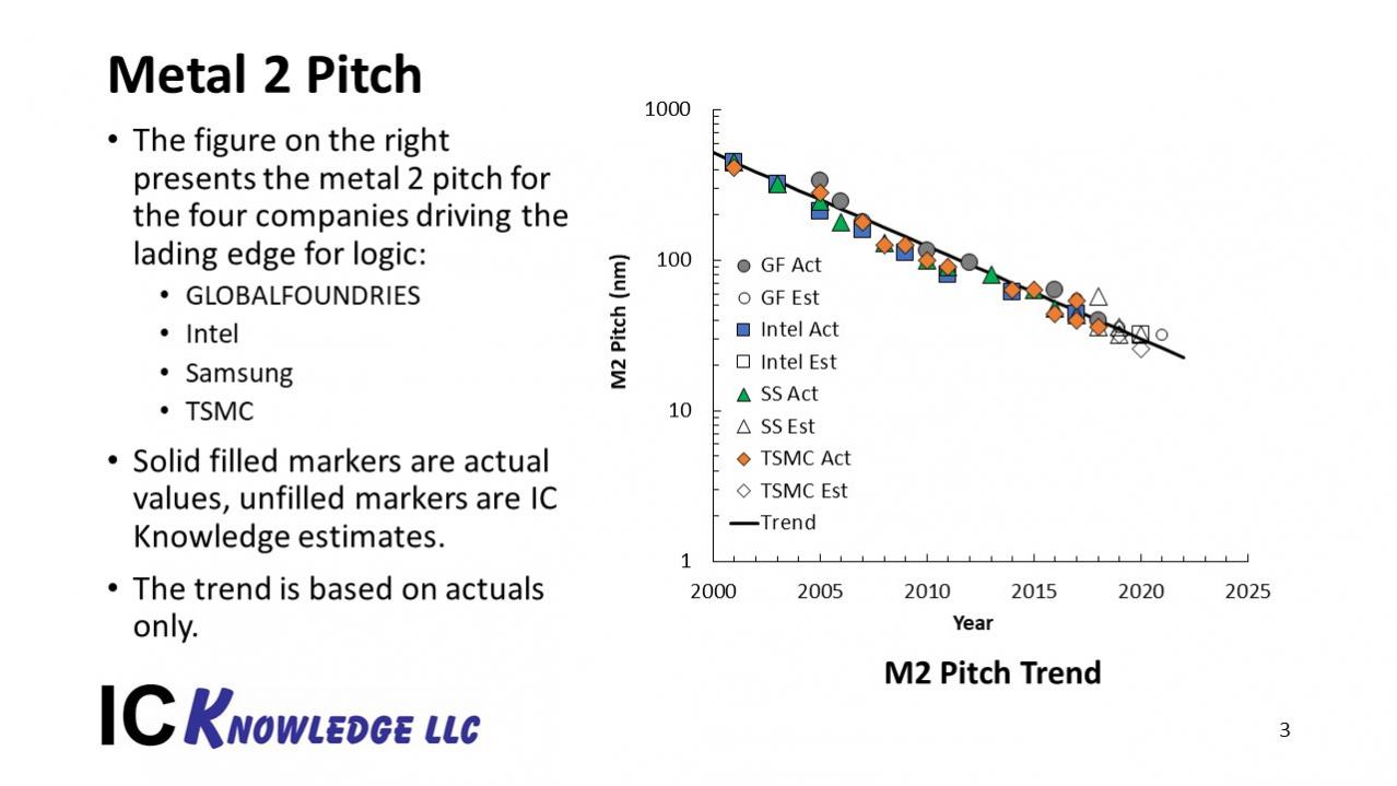
Slide 3. Metal 2 Pitch.
Track Height
In our earliest attempts to define standard cells we used CPP x MMP to define standard cells based on some work ASML did. This work ignored track heights and track heights have become increasingly important with companies pushing down track heights as part of their scaling strategy in what imec calls Design technology Cooptimization (DTCO).
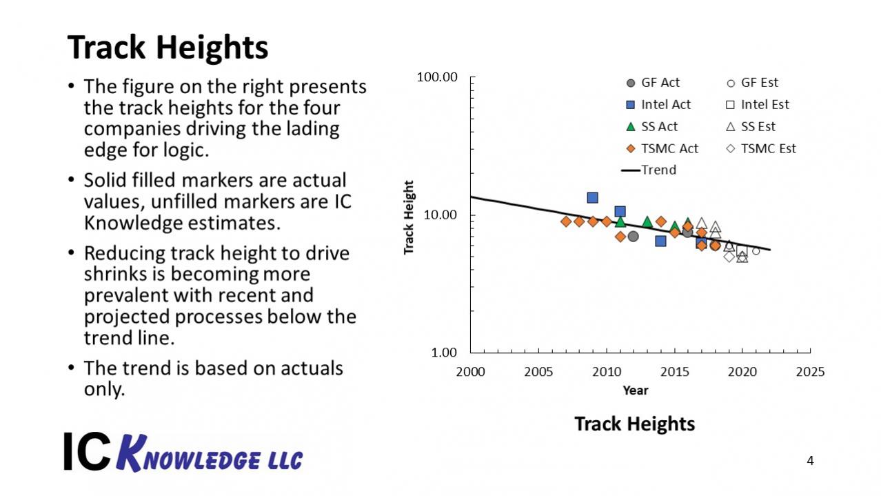
Slide 4. Track Heights.
Using tracks height as part of a scaling strategy is referred to as DTCO because as track height is reduced so is the number of fins per device. Reducing fins per device reduces drive current and performance unless other enhancements are introduced.
Cell Height
Combining actual M2P and track heights and estimated M2P and track heights the cell height (M2P x Tracks) can be calculated. Slide 5 plots the track height versus time for the four companies of interest.
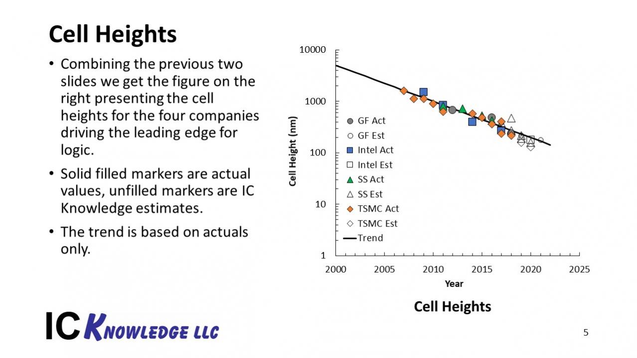
Slide 5 Track Heights.
Cell Widths
Cells widths are some multiple of CPP. The multiple depends on the cell type (more on this in the next two sections and on Double Diffusion Break (DDB) versus Single Diffusion Break (SDB). DDB requires dummy gates at the edges of a cell and for the simple cells illustrated in Slide 6 result in 3x CPP for DDB and 2x CPP for SDB. This is obviously a very important potential area savings although as we will see in a minute for commonly used cells the shrink is much smaller. Even so to get a fair cell size comparison this should be considered.
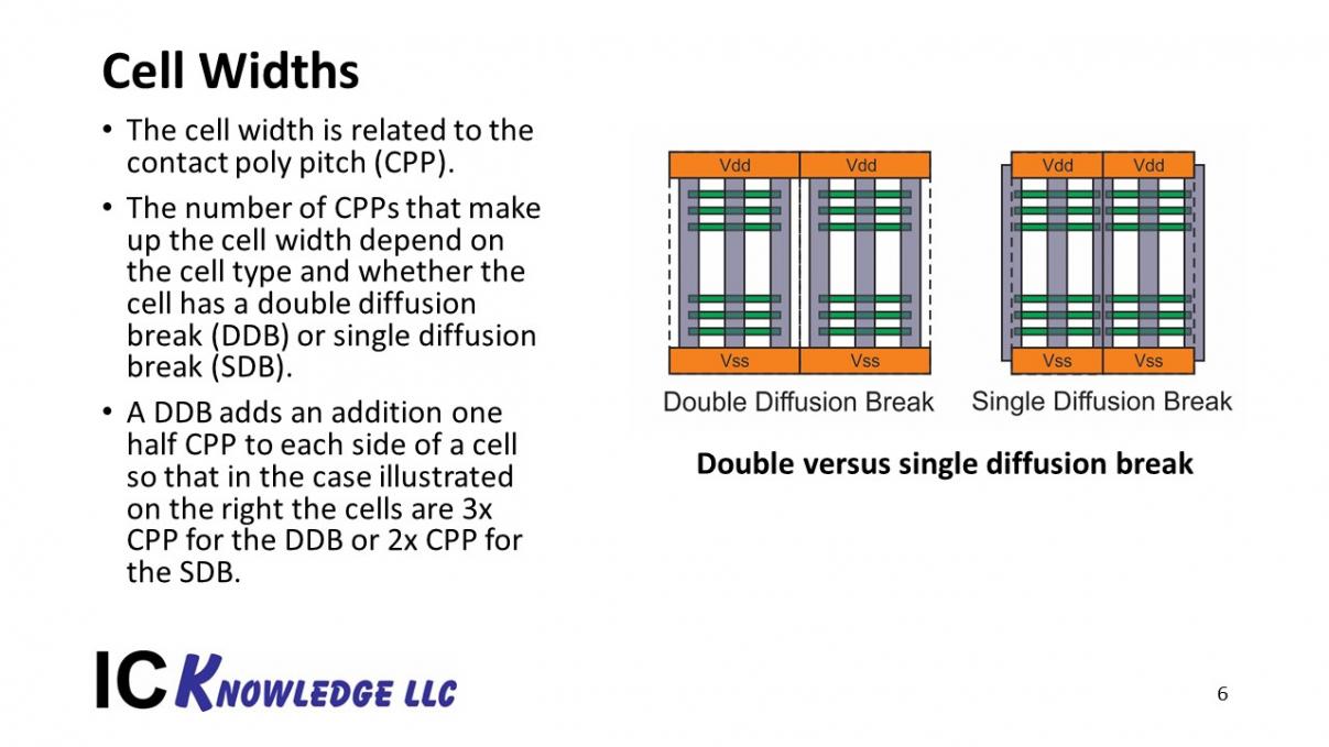
Slide 6. Cell Widths.
Contacted Poly Pitch (CPP)
To calculate cell widths, we need to know the CPP. The CPP is plotted in Slide 8 for the four companies of interest versus time.
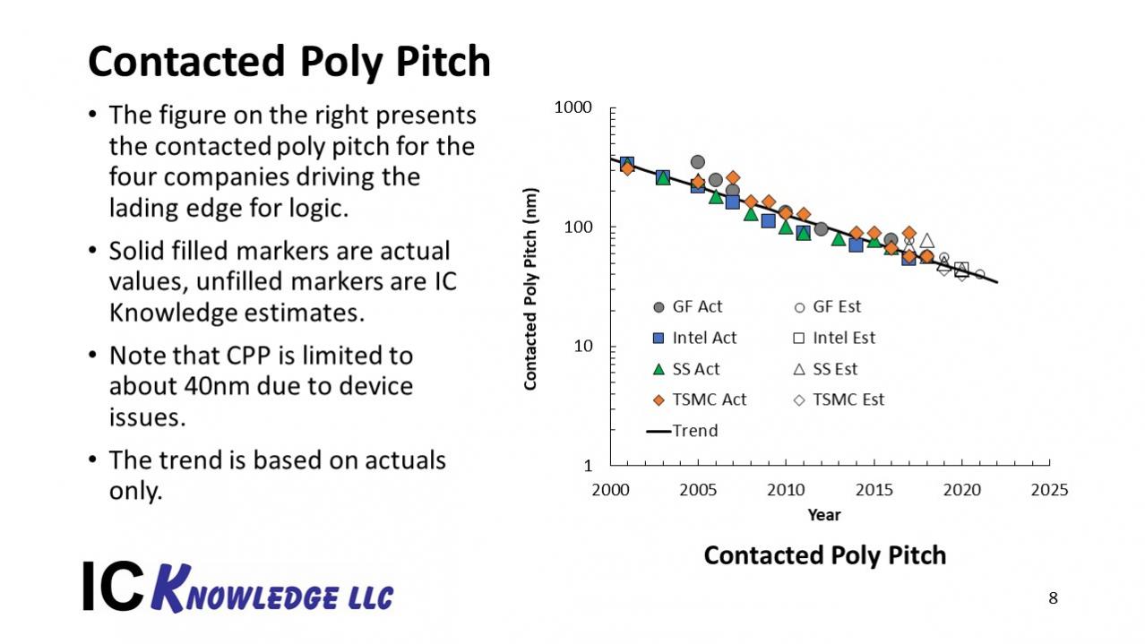
Slide 8. Contacted Poly Pitch.
Comparing Slide 8 (CPP) and Slide 3 (M2P) it can be seen that M2P is scaling more than CPP. CPP is constrained by device issues. See my LithoVision talk written up here for an explanation of the constraints on CPP.
Common Logic Cells
Slide 9 presents a two input NAND cell, one of the most common logic cells. A DDB – two input NAND cell is 4x CPP wide and a SDB two input NAND cell is 3x CPP wide.
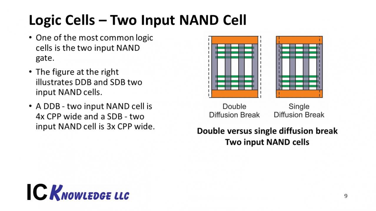
Slide 9. Two Input Logic Cell
Slide 10 presents another of the more common logic cells, the scanned flip flop. A DDB scanned flip flop is 20x CPP wide and a SDB scanned flip flop is 19x CPP wide. A SDB provides more shrink for simpler logic cells.
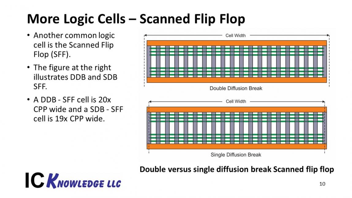
Slide 10. Scanned Flip Flop.
Combining CPP widths from slide 8, the usage of DDB and SDB by process for the leading logic producers and slides 9 and 10 produces 2 input NAND cell width versus time (slide 11) and scanned flip flop cell width versus time slide 12.
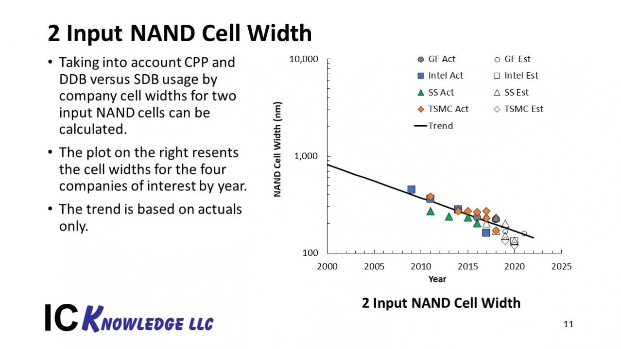
Slide 11. 2 Input NAND Cell Width.
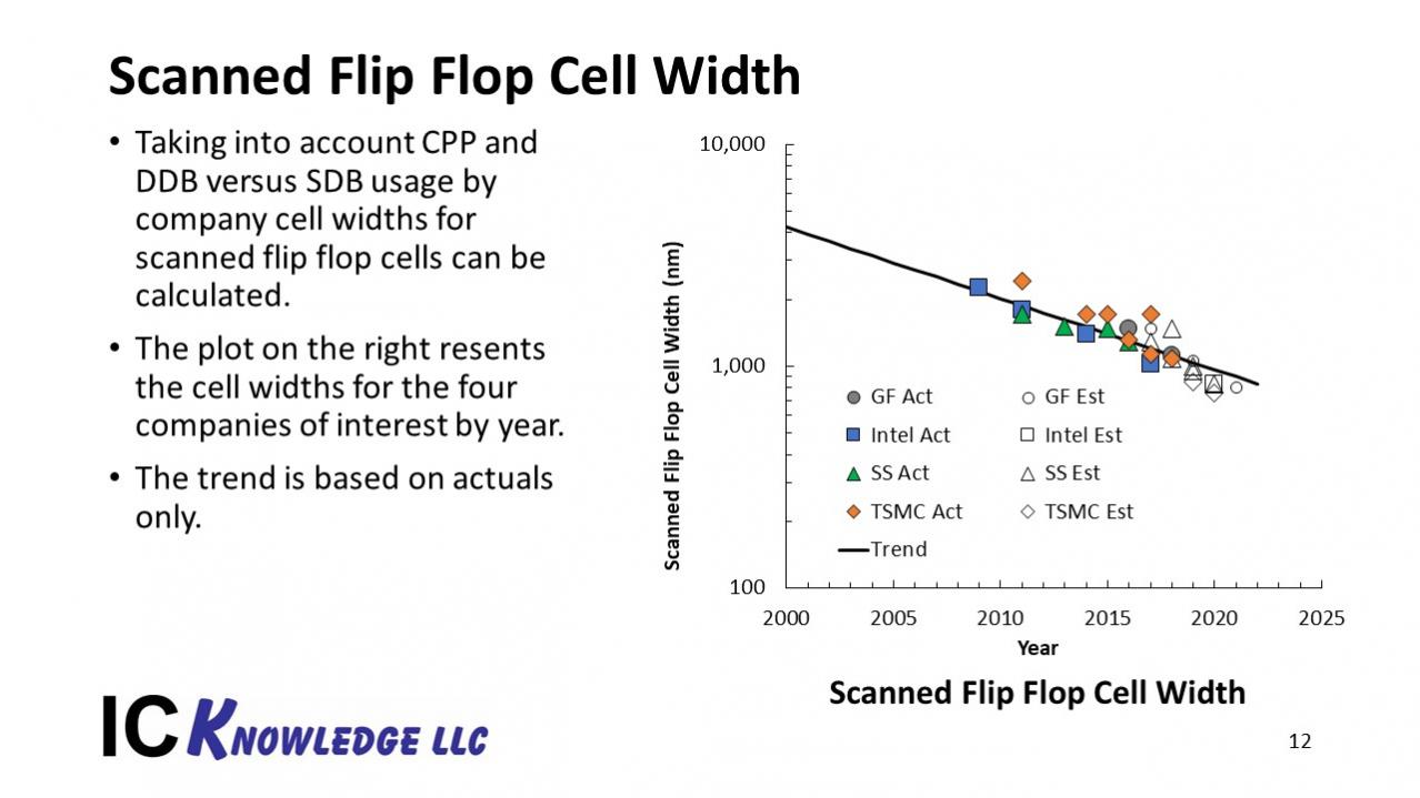
Slide 12. Scanned Flip Flop Cell Width.
Logic Process Density
Intel has proposed a logic process density metric based on calculating transistor density by weighting a two input NAND cell by 60% and a scanned flip flop cell by 40%. The weighting is based on the prevalence of the cells in typical logic designs. A two input NAND cell contains 4 transistors and a scanned flip flop cell contains 36 transistors. Knowing the cell height and widths of two input NAND cells and scanned flip flop cells by company we can plot transistor densities. Slide 14 presents transistor density in millions of transistors per square millimeter versus time for the four companies of interest.
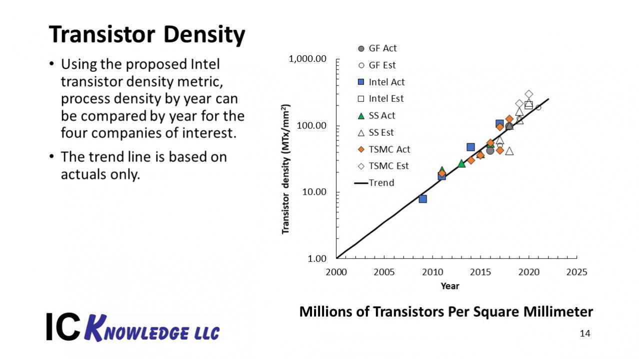
Slide 14. Transistor Density.
Standard Nodes
We could just stop here and compare companies based on transistor density, but as an industry we are used to talking in nodes. Slide 15 plots stated node versus transistor density for the actual process data we have.
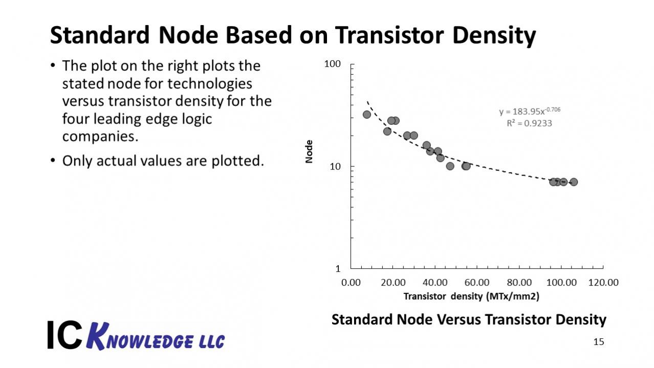
Slide 15. Standard Node Based on Transistor Density.
Using the formula extracted from slide 15 we can plot the standard node trend versus time for the four companies of interest. In cases where a company has multiple processes within a single year we have plotted to densest process.
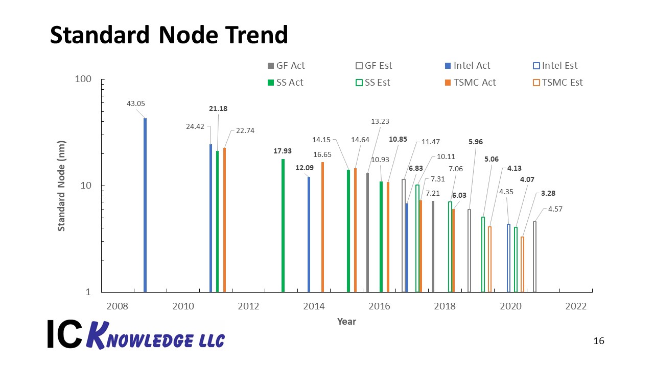
Slide 16. Standard Node Trend.
Conclusion
Adding DDB versus SDB to the standard node discussion makes Intel’s 10nm process slightly denser than first generation 7nm processes but 7nm + processes will move ahead of Intel’s 10nm process in 2019. Looking forward we expect TSMC and Samsung to maintain their lead over Intel for the foreseeable future. GF may also maintain a lead as well, but we have the least visibility into GF’s longer term plans.
The slide deck for this discussion is available here.
Share this post via:


Chemical Origins of Environmental Modifications to MOR Lithographic Chemistry