





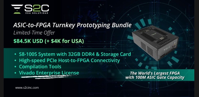
For ASIC design teams, the gap between RTL simulation and first silicon remains one of the most consequential stages of the development cycle. Simulation provides controllability and visibility, but it cannot always reproduce the software workloads, interface behavior, clock interactions, and sustained system activity that expose design problems in a real operating environment. S2C’s ASIC-to-FPGA Turnkey Prototyping Bundle is positioned to close that gap by giving engineering teams a structured route from ASIC RTL to an operational FPGA prototype.
The central value of the bundle is not simply access to FPGA hardware. Its appeal is the combination of prototyping infrastructure, implementation workflow, and technical support required to turn a large ASIC design into a usable validation platform. For teams without a mature in-house prototyping environment, assembling these elements independently can introduce schedule risk. Engineers must select suitable FPGA capacity, partition the design, manage clocking and resets, connect memories and peripherals, resolve FPGA-specific implementation issues, and establish a repeatable debug flow. A turnkey approach aims to reduce that integration burden.
In a typical ASIC-to-FPGA flow, synthesizable RTL is prepared for implementation on one or more FPGAs. ASIC-specific structures, memories, clock-gating logic, and technology-dependent blocks may need to be adapted or replaced with FPGA-compatible equivalents. Large designs must then be partitioned while preserving timing-critical connectivity and minimizing inter-FPGA communication bottlenecks. The resulting implementation must achieve sufficient performance and stability to support meaningful system validation, even though its operating frequency will generally remain below the final ASIC target.
For ASIC designers, the resulting prototype can serve several important purposes. It enables firmware and operating-system development before silicon availability, allowing software teams to boot code, initialize peripherals, exercise drivers, and validate hardware-dependent functions against a physical representation of the design. It also supports long-duration regression tests that may be impractical in simulation, especially when workloads involve billions of cycles, complex protocol traffic, or realistic application software.
A hardware prototype is equally valuable for architectural verification. Engineers can evaluate data movement, memory behavior, interrupt handling, subsystem integration, and interface interoperability under conditions that more closely resemble the final product. Problems involving reset sequencing, asynchronous interactions, system-level deadlocks, or unexpected software-hardware dependencies may become visible earlier, when RTL changes remain possible and less expensive.
Debug capability is therefore a critical consideration. Effective FPGA prototyping requires more than observing a few internal signals. Teams need a disciplined method for selecting probes, capturing events, correlating behavior across partitions, and reproducing failures. Because FPGA resources and trace depth are finite, debug planning should begin before implementation. The strongest turnkey flows help designers balance observability against capacity and timing constraints rather than treating instrumentation as an afterthought.
S2C’s limited-time price of $84.5K USD may be relevant to organizations comparing the cost of a packaged platform with the engineering effort required to build and maintain an internal solution. The economic calculation should include more than the purchase price. Schedule acceleration, earlier software availability, reduced integration effort, improved pre-silicon coverage, and avoidance of a silicon re-spin can outweigh the direct cost of the prototyping environment. Buyers should confirm the exact hardware configuration, FPGA capacity, software licenses, supported interfaces, training, services, delivery terms, and duration of the promotion with S2C.
The bundle is best evaluated against the characteristics of the target ASIC. Important questions include total logic and memory requirements, expected partition count, required external interfaces, prototype performance targets, software workloads, debug objectives, and planned reuse across projects. Teams should also assess how easily the environment fits their existing RTL, verification, version-control, and build processes.
Bottom line: For ASIC programs facing aggressive schedules, S2C’s ASIC-to-FPGA Turnkey Prototyping Bundle offers a way to move system validation, software development, and integration testing earlier in the project. Its real benefit is the opportunity to replace a fragmented setup effort with a coordinated prototyping flow—helping designers reach a stable hardware model sooner and approach tape-out with greater confidence.
Also Read:
COMPUTEX 2026: S2C and Andes Technology Showcase Hardcore “EDA+IP” Synergy for the AI Era
Technical Paper: FPGA Prototyping That Creates Useful PreSilicon Evidence
The “New Shift-Left”: Why FPGA Prototyping is the Ultimate RISC-V IP Sandbox
Share this post via:



Comments
There are no comments yet.
You must register or log in to view/post comments.