

COMPUTEX 2026 officially concluded under the theme “AI Together,” bringing the global semiconductor and computing ecosystem together to showcase the latest advances in artificial intelligence, HPC, and intelligent systems. While AI accelerators and advanced computing platforms dominated the exhibition floor, one collaboration stood out for addressing a critical challenge facing the industry: how to efficiently design and verify increasingly complex AI chips.
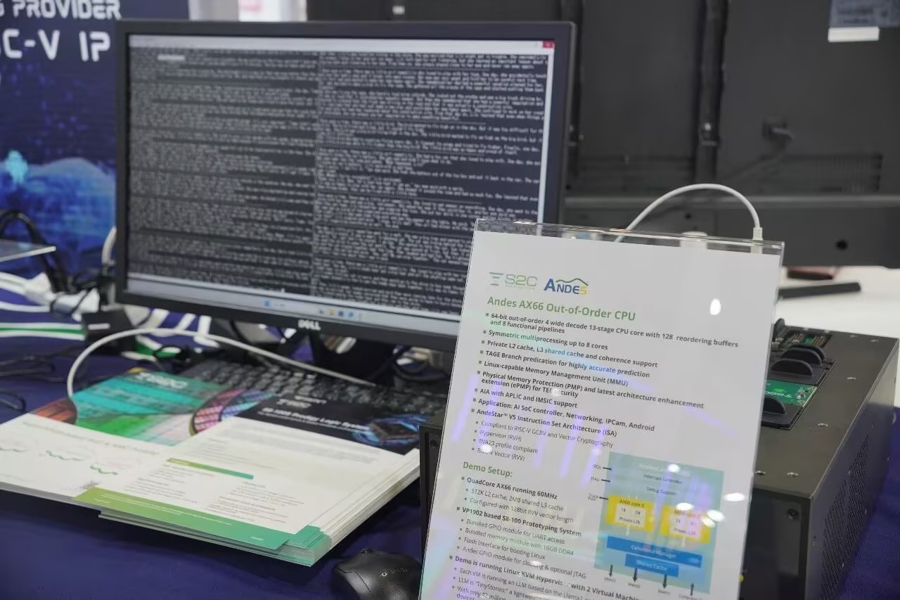
S2C, the world’s largest company focused exclusively on prototyping verification solutions, joined forces with Andes Technology, a leading provider of RISC-V processor IP, to demonstrate how deep integration between EDA platforms and processor IP can accelerate AI innovation. The companies delivered a joint technical presentation and hosted a live demonstration of the Andes AX66 Edge AI platform running on S2C’s flagship Prodigy S8-100 prototyping system.
Solving AI Complexity Through Collaboration
The rapid growth of AI and HPC workloads has dramatically increased SoC complexity. Modern designs routinely incorporate multi-core processor clusters, specialized AI accelerators, and custom instruction extensions. At the same time, chip sizes are approaching hundreds of billions of gates, creating significant challenges for traditional verification and prototyping methodologies.
To address these challenges, S2C and Andes have strengthened their long-term partnership by combining advanced RISC-V processor technology with state-of-the-art FPGA-based prototyping solutions. The goal is to enable engineers to evaluate architectures, validate software, and identify hardware issues much earlier in the design cycle.
At COMPUTEX, the companies showcased this approach through both technical presentations and a real-time AI inference demonstration.
The demonstration featured Andes’ AX66 processor IP, compliant with the latest RVA23 RISC-V standard, implemented on S2C’s Prodigy S8-100 platform. Together, the technologies created a highly integrated hardware emulation environment capable of supporting advanced software workloads.
Running on a Linux KVM virtualization platform, the system launched two virtual machines, each executing a Large Language Model (LLM) based on the Llama2 architecture. The live demo highlighted TinyStories, a lightweight language model containing approximately 42 million parameters. Although modest in size compared to today’s frontier AI models, TinyStories demonstrated how RISC-V processors can efficiently support edge AI applications where power consumption, cost, and deployment flexibility are critical considerations.
The Power of Advanced Prototyping
At the heart of the demonstration was S2C’s latest-generation Prodigy S8-100 prototyping system, powered by the AMD Versal™ Premium VP1902 adaptive SoC. The platform provides approximately 100 million ASIC-gate equivalent capacity per FPGA, making it well suited for validating large-scale multi-core and AI-intensive designs.
As semiconductor designs continue to grow in complexity, single-FPGA solutions often struggle to provide sufficient capacity. S2C addresses this challenge through advanced multi-FPGA prototyping technology and a comprehensive hardware-software co-design environment.
The company’s ecosystem includes tools such as Player Pro, which simplify compilation, design partitioning, and multi-FPGA debugging. These capabilities enable engineering teams to perform deep hardware verification while simultaneously validating operating systems, drivers, middleware, and AI software stacks. By allowing hardware and software development to proceed in parallel, companies can significantly reduce development risk and accelerate time-to-market.
Building a Complete RISC-V Ecosystem
“The explosion of AI, autonomous driving, and HPC applications is pushing chip complexity to unprecedented levels,” said Ying, Vice President of S2C. “When designs reach hundreds of billions of gates, no single company can innovate alone. Customers need complete solutions that help them evaluate architectures, adopt new technologies, and accelerate product development.”
According to Ying, S2C is focused on lowering the barriers to innovation by building an open ecosystem that integrates processor IP, architecture evaluation, software development, and application validation early in the design process.
That strategy is reflected in S2C’s three core strengths: more than two decades of prototyping expertise, close collaboration with leading ecosystem partners such as Andes Technology, and a global support infrastructure that provides localized technical assistance worldwide.
Bottom line: From high-performance multi-core validation to edge AI inference, the S2C-Andes collaboration demonstrates how tightly integrated EDA and IP solutions can help drive the next wave of RISC-V innovation. More importantly, it illustrates a complete methodology centered on ecosystem collaboration, workflow optimization, and early verification—one that can guide advanced AI and RISC-V designs from concept to mass production faster and more efficiently than ever before.
Also Read:
Technical Paper: FPGA Prototyping That Creates Useful PreSilicon Evidence
The “New Shift-Left”: Why FPGA Prototyping is the Ultimate RISC-V IP Sandbox
Accelerating Advanced FPGA-Based SoC Prototyping With S2C
Share this post via:


Comments
There are no comments yet.
You must register or log in to view/post comments.