Synopsys has been acquiring EDA and IP companies at a fast clip over the past few years and it’s often made me wonder how they are going to craft a coherent tool flow for custom IC design. At DACthis year I learned that for schematic capture the winning tool is Custom Designer SE– a relatively new tool, while the IC layout… Read More
 CEO Interview with Dave Kelf, CEO of Breker Verification SystemsIn the functional verification space, Breker Verification Systems stands…Read More
 RISC-V: From Niche Architecture to Strategic FoundationAt the recent RISC-V Now by Andes conference,…Read More
 Bringing mathematical rigour in the world of hardware - a journey into Formal VerificationThis interview presents the first steps of Robert…Read More
 The Great Divide: A Tale of Three Hardware Emulation ArchitecturesHardware emulation arose as a necessity out of…Read More
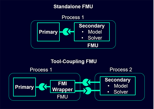
 A Different Angle on Co-Simulation for SystemsCo-simulation, two or more simulations running concurrently in…Read More
Is Your Synchronizer Doing its Job (Part 2)?
In Part 1 of this topic I discussed what it takes to estimate the mean time between failures (MTBF) of a single stage synchronizer. Because supply voltages are decreasing and transistor thresholds have been pushed up to minimize leakage, the shortened MTBF of many synchronizer circuits at nanoscale process nodes is presenting… Read More
TSMC and Xilinx on the FinFAST Track!
The power of the fabless semiconductor ecosystem never ceases to amaze me. On one hand you have the Intel backed press crowing about Intel stealing Altera from TSMC. On the other hand you have Xilinx and TSMC crowing about a new ‘one-team’ approach. If you are interested in the real story you’ve come to the right place.
“Altera’s… Read More
Pat Pistilli: the first cell library, the first computer-printed label and more
At the DAC 50th anniversary banquet, Pat Pistilli won the award for most tenacious attendee, having been to all 50 DACs. Well, and for creating DAC and sustaining it. He was general chair for the first DAC (not yet called DAC) and, of course, would eventually form MP Associates with his wife Marie, which still runs DAC today. In 2010… Read More
Can we really find a way to speed-up Processor & DSP core designs?
Once upon a time, ASIC designers involved in Processor design, like I was, for the first time in 1987 for Thomson CSF and again in 1994 for Texas Instruments, at that time supporting height (8) ASIC designed by another French company, the Advanced Computer Research Institute (ACRI), had to re-invent the wheel almost every day. When… Read More
Agilent ADS Users, Find Out About Design Data Management
In May, ClioSoft and Agilent announced that Agilent’s Advanced Design System (ADS) was now integrated with ClioSoft’s SOS Design Data Management. I interviewed Greg Peterschmidt of Agilent at that time. The information page for the combined product, known as SOS viaADS is here.
Next week ClioSoft is presenting… Read More
DAC by the Numbers
The attendance numbers for DAC are out. Unless you have been living under a stone you know that DAC was in Austin Texas a couple of weeks ago. Attendance was:
- full conference passes: 1589
- exhibits-only passes: 2364
- booth staff: 1998
The registration is slightly lower than last year when DAC was in San Francisco (as it will be again … Read More
SEMICON West: My Top Picks
I will be at Semicon West from 9th to 11th July in Moscone, San Francisco. Of course there are lots of interesting sessions but here are two that I think are especially important to get a good impression of the way things are going in the future from experts. The two most interesting questions about the future are what comes after 14nm,… Read More
What does 3D IC, FinFETs, and EUV have in common?
They are three of the top trending terms on SemiWiki and three of the hot topics at this year’s Semicon West:
In its 43rd year, SEMICON West is the flagship annual event for the global microelectronics industry. It is the premier event for the display of new products and technologies for microelectronics design and manufacturing,… Read More
Static Low-Power Verification in Mixed-Signal SoC Designs
IC designer Shubhyant Chaturvediof AMD used EDA tools from Mentor Graphicsand Concept Engineeringto perform static, low-power verification of a mixed-signal SoC design with a combined CPU and GPU. Shubhyant presented a poster session at DAC two weeks ago in Austin, and I wanted to share it with my readers here at SemiWiki.… Read More


The Semiconductor Growth Numbers are Insane but the Real World Doesn’t Tally!