You are currently viewing SemiWiki as a guest which gives you limited access to the site. To view blog comments and experience other SemiWiki features you must be a registered member. Registration is fast, simple, and absolutely free so please,
join our community today!
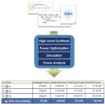
It is so widely accepted that it is already a cliche to say that “power is the new timing.” With more and more chips, the major challenge is not so much to meet timing but to meet timing without blowing out the power budget. Otherwise, you could just crank up the clock rate.
I’m going to be lazy so you can insert your … Read More
The announcement today that Intel will be a Foundry for Altera at 14nm is a significant turning point for the Semiconductor Industry and Intel’s Foundry fortunes of which the full ramifications are not likely to be understood by analysts. As a long time follower of Intel and a former co-founder of an FPGA startup (Cswitch), it has… Read More
In the 1980s, Japan was seen as the leader in the semiconductor industry. Their quality was higher, especially in memories, and the US was worried about falling behind. In fact Sematech was created in 1987 by the US government and a consortium of 14 US-based semiconductor companies primarily to pool investment on common problems… Read More
Nothing seems to raise the Visceral Ire of Semiwiki readers like the two words: Intel and Foundry. To get maximum steam coming out of the ears make sure you combine the two words in a sentence. Something along the lines like: Intel is Now Going to be a Leader in the Foundry Business. Pause…..Ok catch your breadth and now let’s move on … Read More
I recently blogged about the actions filed by Tela Innovations at both the US International Trade Commission (USITC) and in federal district court. Those actions allege that five mobile phone manufacturers -HTC, LG, Motorola Mobility, Pantech, and Nokia – were importing handsets into the US which infringed on seven of… Read More
How do you learn new hardware design topics? I just got trained online about property-based verification for hardware designers using a free online class at Aldec. The material was created by Jerry Kaczynski, a Research Engineer at Aldec.
… Read More
At DAC 2012 we were hearing about the 20nm design ecosystem viability, however IC process technology never stands still so we have early process development going on now at the 10nm and 14nm nodes where FinFET technology is being touted. Earlier in February Vassilios Gerousis, a distinguished engineer at Cadence presented a session… Read More
By now, you will have seen several postings about all the different activities that are going on at Design and Verification Conference being held Feb. 25-28 at its usual location – the DoubleTree Hotel in San Jose, CA. Besides organizing an experts panel “Where Does Design End and Verification Begin?“, Real… Read More
Like Guiness dark beer, competition is good for you! I mean good for end user, as it pushes DSP IP supplier to provide ever better solution. I am not talking about me-to type of competition, like that we have seen in the past with IBM trying to displace TI at Nokia, by offering a LEAD (DSP IP core from TI used in every NOKIA wireless phone… Read More
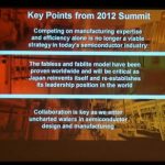
The fabless revolution in the digital semiconductor industry is no more, with just a few integrated device manufacturers (IDMs) remaining on the playing field, it is now the normal way to do business. However, the learning curve for each new process node continues as it always has, with a host of new technical challenges for the … Read More


TSMC N3 Process Technology Wiki