I talked last week about the internet of things (IoT) panel I attended at DAC. One thing that is clear is that IoT is not really a market on its own, but nonetheless the fact that billions of edge-node devices are going to be connected to the internet is a real trend. One company that takes IoT very seriously is Atmel, since they have an … Read More
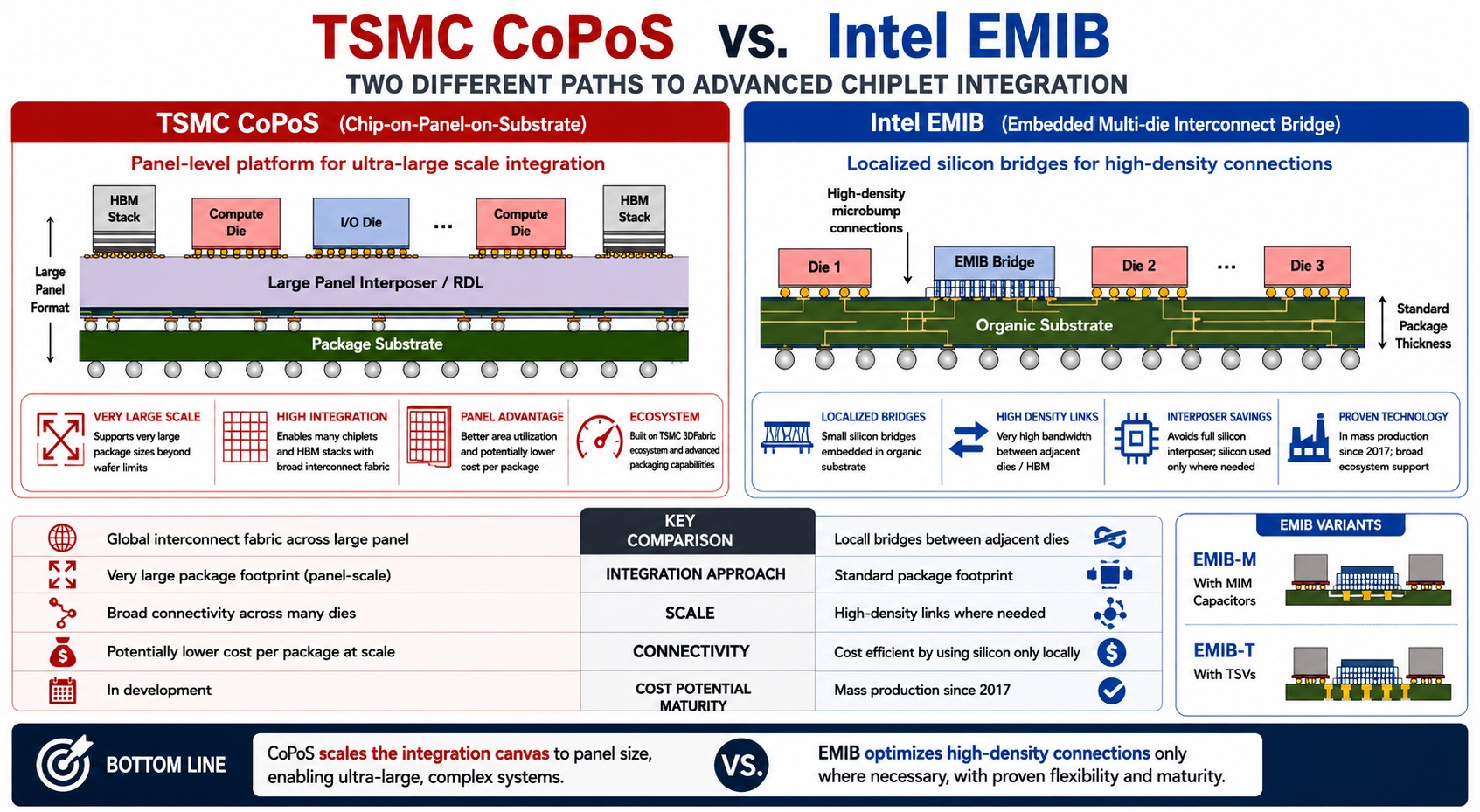 TSMC CoPoS Versus Intel EMIB Semiconductor PackagingTSMC’s CoPoS, generally described as Chip-on-Panel-on-Substrate, and Intel’s…Read More
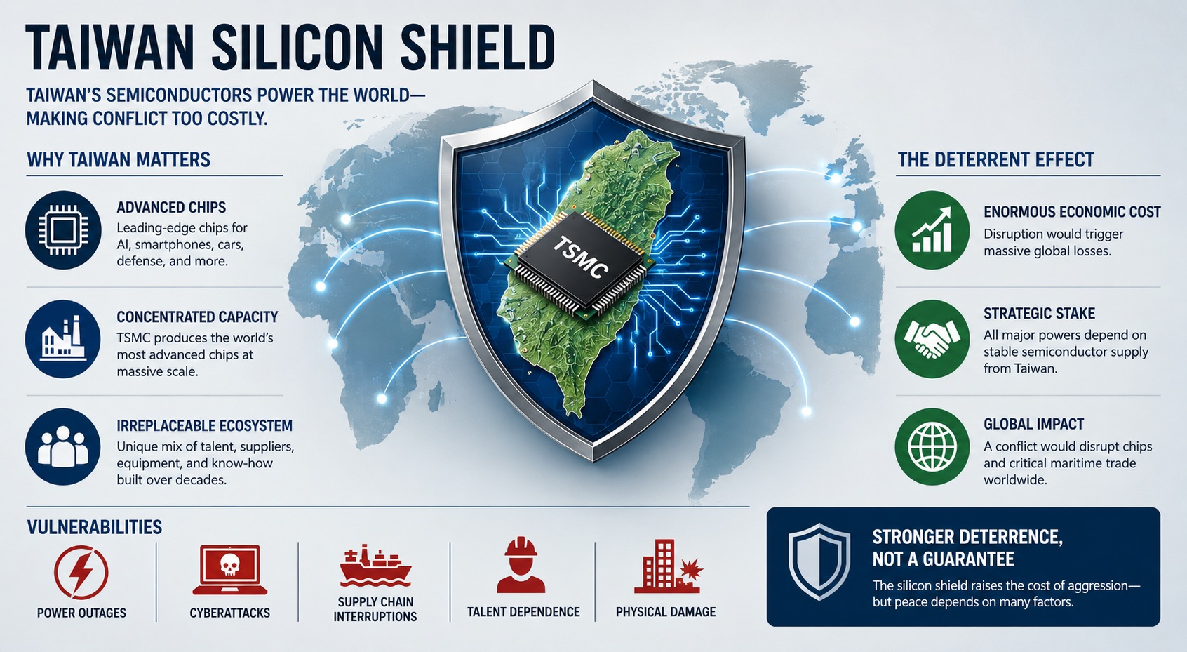 The Silicon Shield Has Never Been Stronger!The “Silicon Shield” describes the idea that Taiwan’s…Read More
 Agentrys Designs a Real Chip with its Multi-Agent WorkforceThe face of EDA is changing. For forty…Read More
 Must-See DAC Panel – Build vs Buy: Who Owns the Intelligence Behind Tomorrow's Chips?This year, DAC will be buzzing about AI…Read More
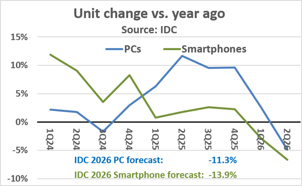
Mobile: China Rising
The mobile numbers for Q1 are now published. At #1 as always is Samsung, who shipped 86M phones for 30% market share. At #2, with almost half as much volume, is Apple who shipped 44M phones. Round here in silicon valley pretty much everyone has either a Samsung Galaxy or an iPhone so you don’t get any sense of who the other major … Read More
An Update on Calibre at DAC
Even though I live just 7 miles away from the Mentor Graphics corporate office in Oregon, I visited their DAC suite in San Francisco last week to get an update on Calibrefrom Michael White. The Calibre tools are used during IC verification and sign-off by performing DRC (Design Rule Checking) and LVS (Layout Versus Schematic).… Read More
A Re-look at TI’s Businesses, Strategies & Future
In recent days I’ve seen several long discussions about Texas Instrumentslosing its grip in semiconductor industry when it came out of a business it was strong in, i.e. wireless business. It seems the semiconductor community has not digested the fact that TI, very rightly, came out of the OMAP business at the right time. The smartphone… Read More
TSMC vs Intel vs Samsung FinFETs
By definition the pure-play foundry business model separates the design and manufacturing of a semiconductor device. TSMC was the first dedicated (pure-play) foundry which enabled the incredible fabless semiconductor ecosystem we have today. If not for the fabless business model we would not have the supercomputer class … Read More
Hogan’s Internet of Things Panel
Jim Hogan organized a panel on the Internet of Things (IoT) on Wednesday afternoon. The panellists were Randy Smith of Sonics, Bernard Murphy of Atrenta, Gary Smith (himself) and Frank Shirrmeister of Cadence.
Gary reckons that IoT is a Wall Street buzzword being used to get stock prices up. If you go to a series of presentations … Read More
Seen at DAC! Self-Driving Cars –Victory Lap or Pile-Up?
It is axiomatic that the DAC vendor community would love to serve the exciting and expanding automotive market; and the auto community would love to continue to increase their value through innovative software/ hardware solutions, which will one day lead to the self-driving car. But how do we team to lap the track?
Jim Hogan set … Read More
The Best and Worst of #51DAC!
When people ask which DAC is the most memorable I used to say my first because I was a new college grad and it really was exciting. The next DAC was memorable since it was in Las Vegas and my beautiful wife joined me. This year was DAC number 30 for me and of course it will be the most memorable since I signed hundreds of copies of “Fabless: … Read More
Embedded Vision Summit

I was a the embedded vision conference last week. Jeff Beir, the founder of the embedded vision alliance gave an introduction to the field. The conference was much bigger than previous years and almost everyone is designing some sort of vision product. Half of your brain is used for vision so it goes without saying that vision requires… Read More
SystemC: User Group update from DAC
I always enjoy attending the SystemC User group to see what is being done by users of SystemC. This time was no exception. Not only is it FREE, but the professional networking around the meeting, presentations, and break times are terrific.
There were 5 paper presentations at the North American SystemC User Group (NASCUG) on Monday,… Read More
Enhancing Multi-Domain System Simulation with FMI Co-Simulation