

Pass the cigars! On November 3rd, 2014, the IEEE-SA Standards Board finally approved IEEE P1687 as a new standard. From now on, you can drop the “P” and just call it 1687, or to its friends, IJTAG. Now would be a good time to sign up for an IJTAG technical workshop.
The new IEEE 1687 Internal JTAG (IJTAG) standard is changing… Read More
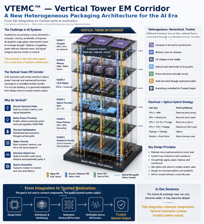
RISC-V and AI: The Architecture Shift Is Now