Developing a localized supply chain for advanced packaging equipment is critical for keeping pace with customers’ increasingly shrinking time-to-market cycles for new artificial intelligence (AI) chips, Taiwan Semiconductor Manufacturing Co (TSMC, 台積電) said yesterday.
Spurred on by the AI revolution, customers are accelerating product upgrades to nearly every year, compared with the two to three-year development cadence in the past, TSMC vice president of advanced packaging technology and service Jun He (何軍) said at a 3D IC Global Summit organized by SEMI in Taipei.
These shortened cycles put heavy pressure on chipmakers, as the entire process — from chip design to mass production — must now be condensed into a single year, He said.
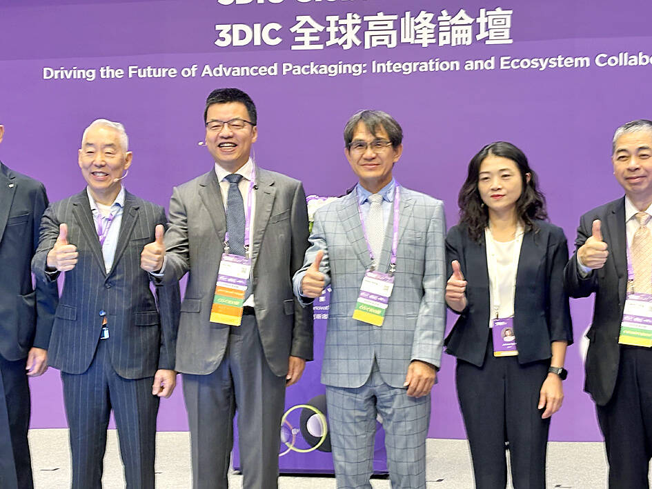 TSMC vice president of advanced packaging technology and service Jun He, second left, and other guests gesture at an 3D IC global summit in Taipei yesterday. Photo: Grace Hung, Taipei Times
That requires TSMC to ramp up production from zero to peak levels in just three quarters, a 30 percent reduction in the time needed to reach high-volume manufacturing, He said, citing the company’s experience over the past three years producing AI chips using its chip-on-wafer-on-substrate (CoWoS) advanced packaging technology.
TSMC must also maintain yield rates of more than 90 percent to avoid financial losses, since the growing integration of components onto a single chip means even minor defects can result in significant value losses, He said.
TSMC consumes about 10 million high-bandwidth memory (HBM) chips each quarter, He said, citing their central role in AI chip production.
To meet such challenges, TSMC must work closely with partners in the local ecosystem, he said. That need also motivated the company’s launch of the 3D IC Advanced Manufacturing Alliance, first proposed last year and officially inaugurated yesterday.
In the past, TSMC had to procure and install advanced packaging equipment before new chip designs were finalized, leading to frequent adjustments, he said.
“Under such circumstances, localization becomes critically important,” He said, adding that research and development teams from both local and global suppliers are required to be involved early in the development process alongside TSMC’s production teams.
He said that about half of chip development is completed several months before mass production begins.
“So, a localized ecosystem is of the utmost importance,” he said.
The advanced packaging business is “not for the faint-hearted,” given its combination of high risks and high returns, he added.
The global advanced packaging market is forecast to grow at an annual rate of 12.7 percent, reaching US$79 billion by 2030, up from US$38 billion last year, fueled by surging demand for AI applications, Yole Intelligence forecast.
To meet this demand, TSMC has more than doubled its CoWoS capacity over the past two years. CoWoS technology is used to package AI chips
Local advanced packaging equipment suppliers — including ASE Technology Holding Co (日月光投控), Chroma ATE Inc (致茂), Grand Process Technology Corp (弘塑科技) and C Sun Manufacturing Ltd (志聖) — are among the 37 members of the newly established 3D IC Advanced Manufacturing Alliance.
 www.taipeitimes.com
Spurred on by the AI revolution, customers are accelerating product upgrades to nearly every year, compared with the two to three-year development cadence in the past, TSMC vice president of advanced packaging technology and service Jun He (何軍) said at a 3D IC Global Summit organized by SEMI in Taipei.
These shortened cycles put heavy pressure on chipmakers, as the entire process — from chip design to mass production — must now be condensed into a single year, He said.
That requires TSMC to ramp up production from zero to peak levels in just three quarters, a 30 percent reduction in the time needed to reach high-volume manufacturing, He said, citing the company’s experience over the past three years producing AI chips using its chip-on-wafer-on-substrate (CoWoS) advanced packaging technology.
TSMC must also maintain yield rates of more than 90 percent to avoid financial losses, since the growing integration of components onto a single chip means even minor defects can result in significant value losses, He said.
TSMC consumes about 10 million high-bandwidth memory (HBM) chips each quarter, He said, citing their central role in AI chip production.
To meet such challenges, TSMC must work closely with partners in the local ecosystem, he said. That need also motivated the company’s launch of the 3D IC Advanced Manufacturing Alliance, first proposed last year and officially inaugurated yesterday.
In the past, TSMC had to procure and install advanced packaging equipment before new chip designs were finalized, leading to frequent adjustments, he said.
“Under such circumstances, localization becomes critically important,” He said, adding that research and development teams from both local and global suppliers are required to be involved early in the development process alongside TSMC’s production teams.
He said that about half of chip development is completed several months before mass production begins.
“So, a localized ecosystem is of the utmost importance,” he said.
The advanced packaging business is “not for the faint-hearted,” given its combination of high risks and high returns, he added.
The global advanced packaging market is forecast to grow at an annual rate of 12.7 percent, reaching US$79 billion by 2030, up from US$38 billion last year, fueled by surging demand for AI applications, Yole Intelligence forecast.
To meet this demand, TSMC has more than doubled its CoWoS capacity over the past two years. CoWoS technology is used to package AI chips
Local advanced packaging equipment suppliers — including ASE Technology Holding Co (日月光投控), Chroma ATE Inc (致茂), Grand Process Technology Corp (弘塑科技) and C Sun Manufacturing Ltd (志聖) — are among the 37 members of the newly established 3D IC Advanced Manufacturing Alliance.
Local ecosystem key to meeting AI demand: TSMC - Taipei Times
Bringing Taiwan to the World and the World to Taiwan