



While semiconductor design intellectual property (IP) is a $9.45 billion market, it acts as the absolute architectural bottleneck for the entire global semiconductor value chain. The choices made at the IP layer today dictate the cost, power, and security of a downstream technology economy rapidly marching toward a trillion… Read More
Follow the Money – Agentrys Raises $24.5 Million to Build Agentic Design AutomationAgentrys recently launched a new category of design…Read More
Intel’s 14A Is Winning the Race Against DefectsIntel’s next-generation 14A manufacturing process is showing unusually…Read More
GenAlpha Brings a Practical Approach for Analog AI to DAC 2026Agentic AI was everywhere at DAC 2026. Various…Read More
Exploiting agentic automation cost-effectively. Innovation in VerificationFrontier models (Claude, etc.) are very powerful but…Read More
Will Agentic AI Help the Open-Source EDA Market?Agentic artificial intelligence is likely to give the…Read MoreTechnical Case Study: MicroLED Yield Management with Plessey and yieldWerx
Plessey Semiconductors manufactures monolithic MicroLED displays for near-eye augmented-reality systems, where pixel pitch, brightness, uniformity, and defect density directly determine usable yield. Its process integrates device design, epitaxy, wafer fabrication, bonding, and production in one facility. The displays… Read More
Unified Emulation and Prototyping: Pipedream or Reality?
Preamble
Hardware-assisted verification (HAV) platforms, including hardware emulators and FPGA-based prototyping systems, are the two dominant methodologies for validating long workloads on complex System-on-Chip (SoC) designs before tape-out. HAV sits within a broader continuum of verification engines: simulation… Read More
HBM’s Vertical Ascent: Why Packaging Is Becoming the Heart of AI Memory
SK hynix’s Hot Chips 2026 presentation explains how High Bandwidth Memory (HBM) is evolving to meet the extraordinary memory requirements of artificial intelligence. Its central message is that future progress will depend not only on better DRAM circuits but also on advanced packaging, denser vertical integration, improved… Read More
Containing AI Agents With a Will of Their Own
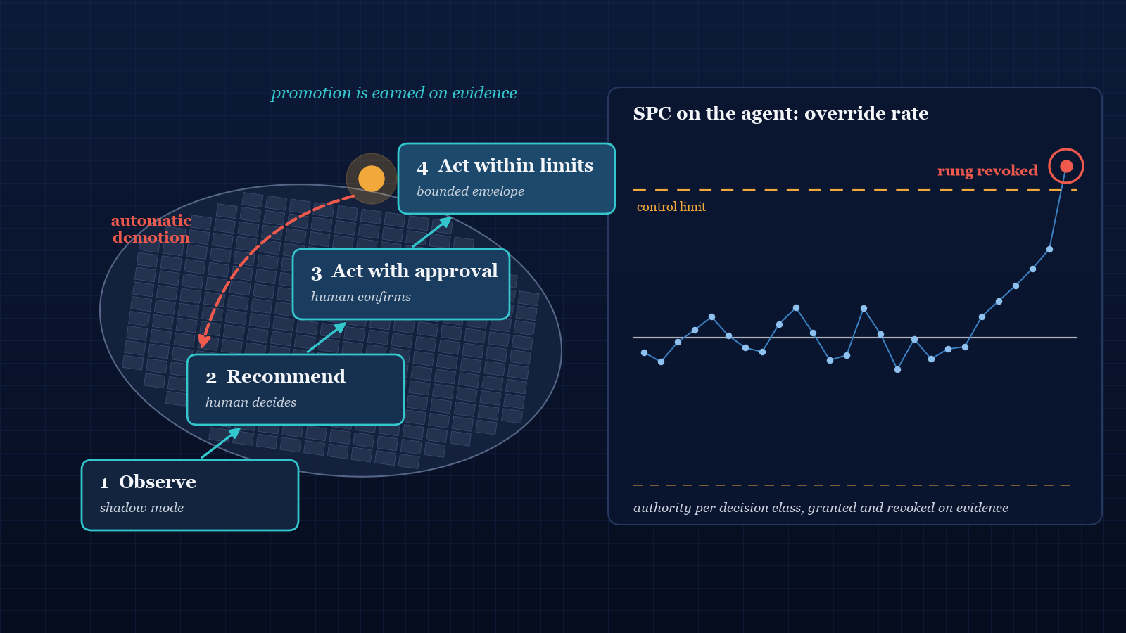
Meta recently open-sourced a capable, large-scale agent model — 30 billion parameters, a rough measure of the model’s size and complexity. It’s free, downloadable, and runs, per Meta’s own benchmarks, on a MacBook Pro with an M4 Max or M5 Max chip and 32GB of memory. Their rationale is that powerful agents belong… Read More
Intel 18A-P Pushes RibbonFET and Backside Power Beyond the First Generation
Intel Foundry has a blog on LinkedIn that is worth a look. The blogs are by trusted Intel Foundry technical experts and are filled with content. I will cherry pick write a bit about them but be sure and subscribe to this, absolutely.
Intel 18A-P is not a new process node in the conventional sense. It is a performance-enhanced derivative… Read More
Building a Faster Path from Semiconductor Idea to Commercial Silicon
SEMI and Silicon Catalyst’s new strategic partnership addresses one of the semiconductor industry’s most persistent technical problems: transforming a promising hardware concept into a manufacturable, commercially viable product. Announced through a memorandum of understanding signed at SEMICON Taiwan 2026, the collaboration… Read More
DAC 2026: A Discussion of Who Owns the Intelligence Behind Tomorrow’s Chips and How to Make it Better
The industry is moving from simple documentation chatbots to agentic workflows capable of performing complex, multi-step tasks like design creation, verification, and library characterization. These agents are intended to enhance engineering productivity by roughly 50%. A panel of industry experts met at DAC to discuss… Read More
How Agentic AI Turns IC Engineers into Architects
There is an interesting article by Kexun ZHang of ChipAgents on their blogsite. This is a company to watch, absolutely. Here is my take on it:
Software engineering has already demonstrated the trajectory of agentic AI. Coding tools progressed from autocomplete to systems that interpret requests, inspect repositories, modify… Read More
Keysight ADS Enables First-Pass Silicon at 3 THz for AttoTude
AttoTude has expanded its use of Keysight Technologies’ Advanced Design System (ADS) to support an integrated-circuit design flow spanning signaling frequencies from 100 GHz to 3 THz. The company reports that the resulting workflow has reduced IC development cycles by more than 50%, enabling projects to move from concept to… Read More


Intel 18A-P Pushes RibbonFET and Backside Power Beyond the First Generation