At the 2023 SPIE Advanced Lithography and Patterning conference, ASML presented an update on its EUV lithography systems in the field [1]. The EUV wafer exposure output was presented and is shown below in table form:

From this information, we can attempt to extract and assess the EUV wafer output per quarter. First, since there are quarters with no reported output, we will interpolate with a quartic polynomial fit. A quartic polynomial is used as best fit because five data points are already available.

Cumulative EUV wafers exposures from 2019 to 2022. Quarter 0 corresponds to before Q1 2019.
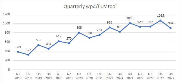
For each quarter, we can calculate the average wafers per day per EUV tool, by taking the difference between wafers exposed in a pair of consecutive quarters, dividing by the average of the number of available systems of the two quarters, then dividing by 90 days. The resulting trend is shown below:

Average wafers per day per EUV system, for each quarter from 2019 to 2022.
The average EUV exposures per tool broke through 1000 wafers per day in a couple of quarters, but has most recently dropped to 904 wafers per day, or less than 40 wafers per hour. This looks like a surprisingly low throughput, compared to reported values of 120-180 wafers per hour [1], what could this mean?
A first possibility is that the EUV tools are simply not used that often, and are idle most of the time. A second possibility is that the tools are in maintenance most of the time. However, uptime of >90% has been reported [2]. A third possibility would be higher doses, possibly over 100 mJ/cm2, to address stochastic effects [3]. However, this does seem to go counter to all the work done on achieving published throughput goals. Yet another possibility is that the graph does not count multiple layer exposures on a wafer separately. Hence, 15 EUV layers at 120 wafers per hour each layer would look like 8 wafers per hour, for example. However, compared to ~40 wafers per hour on average, this number is an even lower output rate! Where is the discrepancy? Research and development (R&D) wafers have not been considered. If only 20% of all EUV wafers run were for production, then the numbers could work out more reasonably. A possible breakdown would be below:

An example of EUV use breakdown for Q4 2022. In this case, uptime is allocated as 20% for production, 20% for R&D, 60% idle. The resulting monthly production volume is 933,333 wafers/month. Production assumed to run wafers at 120 WPH, R&D at 128 WPH.
For reference, TSMC monthly output is reported as up to 150,000 wafers/month [4]. If the monthly production volume is not over 900,000 wafer/month but actually ~250,000 wafers/month (so that TSMC’s portion is 60% of global total), the fraction in production needs to be ~5.3%. With the same wafer run rates, the R&D and idle time fraction don’t change appreciably.

In this example, uptime is allocated as 5.3% for production, 28% for R&D, 67% idle. The resulting monthly production volume is 247,333 wafers/month. Production assumed to run wafers at 120 WPH, R&D at 128 WPH.
The noticeable difference is the number of layers per production wafer. On average, it has increased to 57. This must include the multiple exposures for a given layer for many cases. For example, 14 layers with four exposures, and 1 layer with single exposure, to give 15 EUV layers and 57 EUV exposures total.
In both of the above examples, yield loss is not considered. If we assume that the monthly production volume is actually 420,000 wafers, but that yield loss had brought it down to 250,000, the production use is 9%. The 33 EUV exposures could come from 6 layers with four exposures, and 9 layers with single exposure, to give 15 EUV layers total.

In this example, uptime is allocated as 9% for production, 26% for R&D, 65% idle. The resulting monthly production volume is 420,000 wafers/month. Production assumed to run wafers at 120 WPH, R&D at 128 WPH.
The picture that emerges from considering the above scenarios is that there is substantial (>60%) idle time, some yield loss, and a good deal of multiple exposures (multipatterning) for some EUV layers, if we assume the EUV systems are running at least 120 wafers per hour. Otherwise, if the tools are not idle or under maintenance or repair for that much time, the actual running throughput is often (on average) <40 wafers per hour. Very high doses to address stochastic effects naturally result in such low throughputs.
References
[1] C. Smeets et al., Proc. SPIE 12494, 1249406 (2023).
[2] https://semiengineering.com/euv-challenges-and-unknowns-at-3nm-and-below/
[3] https://semiengineering.com/finding-predicting-euv-stochastic-defects/
[4] https://www.digitimes.com/news/a20220323PD215.html
This article first appeared in LinkedIn Pulse: Assessing EUV Wafer Output: 2019-2022
Also Read:
Application-Specific Lithography: 28 nm Pitch Two-Dimensional Routing
SPIE 2023 – imec Preparing for High-NA EUV
Curvilinear Mask Patterning for Maximizing Lithography Capability
Share this post via:


Is Intel About to Take Flight?