You are currently viewing SemiWiki as a guest which gives you limited access to the site. To view blog comments and experience other SemiWiki features you must be a registered member. Registration is fast, simple, and absolutely free so please,
join our community today!
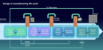
Preventing the propagation of systematic defects in today’s semiconductor design-to-fabrication process requires many validation, analysis and optimization steps. Tools involved in this process can include design rule checking (DRC), optical proximity correction (OPC) verification, mask writing and wafer printing… Read More
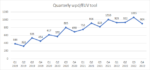
At the 2023 SPIE Advanced Lithography and Patterning conference, ASML presented an update on its EUV lithography systems in the field [1]. The EUV wafer exposure output was presented and is shown below in table form:
From this information, we can attempt to extract and assess the EUV wafer output per quarter. First, since there … Read More
The Siemens Calibre group was very busy last week at SPIE. Calling Calibre industry leading really is an understatement. Calibre is one of the reasons Moore’s Law has continued to this day. This tool is legendary. You can get more information on the Calibre landing page including product information, resource guide, blogs
…
Read More