Array
(
    [content] => 
    [params] => Array
        (
            [0] => /forum/index.php?threads/will-vtfet-become-the-new-chip-technology.18763/
        )

    [addOns] => Array
        (
            [DL6/MLTP] => 13
            [Hampel/TimeZoneDebug] => 1000070
            [SV/ChangePostDate] => 2010200
            [SemiWiki/Newsletter] => 1000010
            [SemiWiki/WPMenu] => 1000010
            [SemiWiki/XPressExtend] => 1000010
            [ThemeHouse/XLink] => 1000970
            [ThemeHouse/XPress] => 1010570
            [XF] => 2021370
            [XFI] => 1050270
        )

    [wordpress] => /var/www/html
)

Will VTFET become the new chip technology?

Arthur Hanson

Well-known member
Any thoughts or insights on this would be appreciated.

IBM and Samsung announce semiconductor design breakthrough​


A Researcher At A Thermal Compression Bonding (tcb) Tool In Nano Fab South At Albany


The global semiconductor chip shortage has led to significant frustration as organizations across many industries have resorted to plan B. However, it has also prompted significant investment in research and development efforts necessary to find new solutions.

Case in point – IBM and Samsung Electronics are jointly announcing a breakthrough that defies conventional semiconductor design and aims to reduce the energy usage of chips by 85 percent or double performance compared to scaled finFET transistors.

Developed by a joint team of researchers at the Albany Nanotech Complex, IBM and Samsung's new VTFET design prototype successfully implements transistors built vertically on the surface of a chip. Because transistors have, until now, been built horizontally to lie flat upon the surface of a semiconductor, this allows an exponential number of transistors to exist on a chip and removes density and energy efficiency constraints.


IBM and Samsung announce semiconductor design breakthrough​

Dec. 14, 2021


New innovation demonstrates a path to scaling beyond the nanosheet.
Peter Fretty
Connie Zhou for IBM

A Researcher At A Thermal Compression Bonding (tcb) Tool In Nano Fab South At Albany

View Image Gallery


The global semiconductor chip shortage has led to significant frustration as organizations across many industries have resorted to plan B. However, it has also prompted significant investment in research and development efforts necessary to find new solutions.

Case in point – IBM and Samsung Electronics are jointly announcing a breakthrough that defies conventional semiconductor design and aims to reduce the energy usage of chips by 85 percent or double performance compared to scaled finFET transistors.
Developed by a joint team of researchers at the Albany Nanotech Complex, IBM and Samsung's new VTFET design prototype successfully implements transistors built vertically on the surface of a chip. Because transistors have, until now, been built horizontally to lie flat upon the surface of a semiconductor, this allows an exponential number of transistors to exist on a chip and removes density and energy efficiency constraints.
“We see high bandwidth communication between chips as advanced interconnect becoming more important in the years to come. Lasers, photonics and optics will have a critical role to play in these innovations,” Huiming Bu - Vice President, Hybrid Cloud Technology Research & Albany Operation, IBM Research tells Laser Focus World. “These adjacent technologies have continued to play an increasing role in system integration, and it is anticipated they would bring complementary values in parallel along with transistor architecture innovations well into the future.”
The VTFET process addresses many barriers to performance and limitations to extend Moore’s Law as chip designers attempt to pack more transistors into a fixed space. It also influences the contact points for the transistors, allowing for greater current flow with less wasted energy. Overall, the new design aims to deliver a twotimesimprovement in performance or an 85 percent reduction in energy use as compared to scaled finFET alternatives.

Connie Zhou for IBM

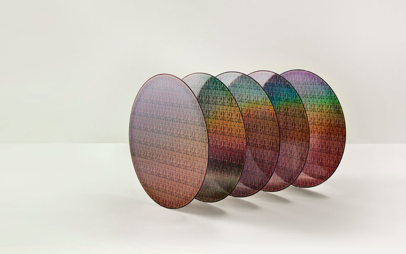
VTFET (Vertical-Transport Nanosheet Field Effect Transistor) wafers

VTFET (Vertical-Transport Nanosheet Field Effect Transistor) wafers​
According to the paper Bu and his associates wrote for IEDM, “At fixed footprint and aggressively scaled gate pitches, VTFET nanosheets can deliver increased device drive due to a combination of good electrostatics, low parasitic losses, and area savings from the use of zero diffusion breaks. VTFET Nanosheets can avoid Lateral FET scaling limits to deliver an enhanced operating voltage range. VTFET Nanosheets can also provide greater drive strength and flexibility compared to FinFETs and Nanowires. The intrinsic benefit of VTFET circuit capacitance reduction (~ 50%) over scaled Lateral FET has been demonstrated in hardware.”

“We believe the areas of EDA, inline metrology and process control (controlling physical parameters along the vertical Z direction in mass production) are areas of rich opportunities for VTFET adoption in the industry,” says Bu. “We are introducing this new device architecture at IEDM this year and hence not associating it to any specific technology node yet. Our intent is to introduce the VTFET architecture with its many advantages and unique features. The actual node adoption is aimed to be after Nanosheet Technology.”
 
VTFET main allure is the "free" path to monolithic 3D, which horizontal devices don't have.

Even two stack VTFET is would be a 2-3 node leap equivalent, even if the baseline device will be larger than FF. And six stack will allow you to have a cell with the footprint of a single transistor, and allow a completely different approach to routing.
 
Like the CFET, it would only help if there is a buried connecting line. If it's all top-access, the benefits may not hold.

But if you can verticalize whole cells, and not run metal in between devices in the cell from the top, benefits are massive.
 
But if you can verticalize whole cells, and not run metal in between devices in the cell from the top, benefits are massive.
You are then mixing BEOL processing and FEOL processing, which is a big fat no no. 3D NAND gets away with it b/c the array is built inside the beol, and the process of making the transistors is different than periphery/logic/dram feols.
 
VTFET main allure is the "free" path to monolithic 3D, which horizontal devices don't have.

Even two stack VTFET is would be a 2-3 node leap equivalent, even if the baseline device will be larger than FF. And six stack will allow you to have a cell with the footprint of a single transistor, and allow a completely different approach to routing.
"VTFET main allure is the "free" path to monolithic 3D, which horizontal devices don't have."

How did you come to the conclusion that this is a stackable technology? It's not clear to me that this is stackable and that isn't what the paper discusses as the advantage of this technology.
 
What is actually different about this compared to GAA/nanosheets? Is it nanosheets but rotated 90 degrees so they're on edge not flat? Or is it just another name for CFET? (NMOS and PMOS stacked vertically)
 
Once you make the change from FinFETs to Horizontal Nanosheets (HNS) you open up a scaling path that will carry us for over ten more years of logic scaling. First there will be multiple generations of HNS, then multiple generations of CFET, and eventually 2D material CFETs. We are currently at less than 300 million transistors/millimeter squared (MTx/mm2) for the densest logic, my calculations are that 2D CFET can get to ~1,500 MTx/mm2. The vertical technology described in the paper is interesting but to my view doesn't offer the scaling path that HNS does. Furthermore if you look at what the three logic leaders are doing they are all on the HNS/CFET/2D path.
 
What is actually different about this compared to GAA/nanosheets? Is it nanosheets but rotated 90 degrees so they're on edge not flat? Or is it just another name for CFET? (NMOS and PMOS stacked vertically
It is nanosheets rotated 90 degrees.

I don't see this as stackable and it isn't a CFET.

It looks to me like the vertical nanosheet would be lithographically defined and that has more variability than the epitaxially defined horizontal nanosheets (HNS).

As I noted above I don't see this as having the scaling path that HNS opens up.
 
"VTFET main allure is the "free" path to monolithic 3D, which horizontal devices don't have."

How did you come to the conclusion that this is a stackable technology? It's not clear to me that this is stackable and that isn't what the paper discusses as the advantage of this technology.

Common channel structure, around which drains gates and sources are built up. The channel itself is either structured first, or deep RIE cut through multiple drain/gate/source layers, and filled in.

First functioning demonstrators of stacked VTFETs were made in research labs decades ago.
 
Furthermore if you look at what the three logic leaders are doing they are all on the HNS/CFET/2D path.
Why FinFET got ahead of VTFET was that it was a more straightforward, and less radical improvement on the existing technology, and HNS is the same.
 
You are then mixing BEOL processing and FEOL processing, which is a big fat no no. 3D NAND gets away with it b/c the array is built inside the beol, and the process of making the transistors is different than periphery/logic/dram feols.
You are already getting into it with burried power, and burried contacts
 
You are already getting into it with burried power, and burried contacts
We’ve had this very discussion before. Every single BSP paper out there uses tungsten not copper. Scotten has talked about resistance from chipmakers on BPR due to the fact that the tungsten gets laid out first. But you must keep in mind if it was copper then this technology would go from challenging to flat out impossible. As far as I remember intel has not talked about when in the flow powervias are made and TSMC has not publicly stated what BSPD scheme they are using.
 
Once you make the change from FinFETs to Horizontal Nanosheets (HNS) you open up a scaling path that will carry us for over ten more years of logic scaling. First there will be multiple generations of HNS, then multiple generations of CFET, and eventually 2D material CFETs. We are currently at less than 300 million transistors/millimeter squared (MTx/mm2) for the densest logic, my calculations are that 2D CFET can get to ~1,500 MTx/mm2. The vertical technology described in the paper is interesting but to my view doesn't offer the scaling path that HNS does. Furthermore if you look at what the three logic leaders are doing they are all on the HNS/CFET/2D path.
What calculations are you basing this assertion on?
 
Back
Top