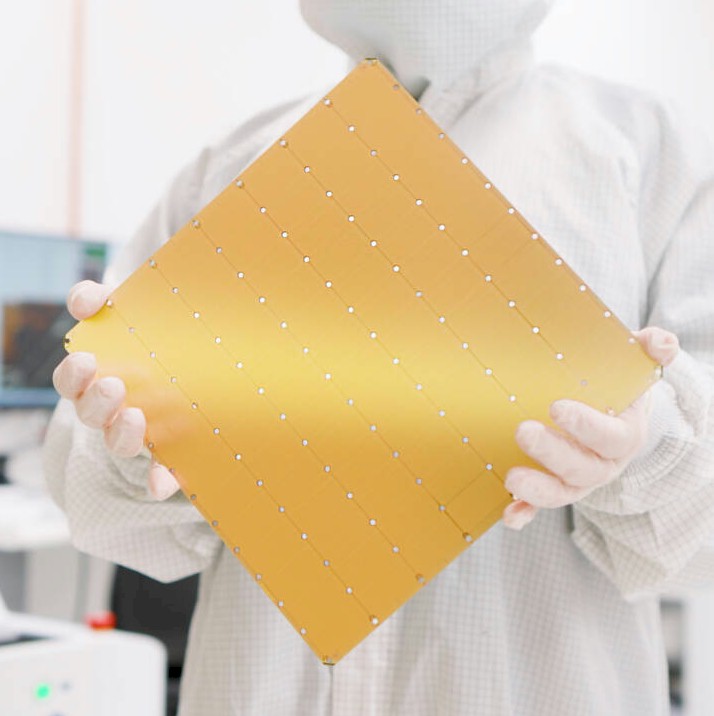
Array
(
    [content] => 
    [params] => Array
        (
            [0] => /forum/index.php?threads/the-new-cerebras-cs-3.19821/
        )

    [addOns] => Array
        (
            [DL6/MLTP] => 13
            [Hampel/TimeZoneDebug] => 1000070
            [SV/ChangePostDate] => 2010200
            [SemiWiki/Newsletter] => 1000010
            [SemiWiki/WPMenu] => 1000010
            [SemiWiki/XPressExtend] => 1000010
            [ThemeHouse/XLink] => 1000970
            [ThemeHouse/XPress] => 1010570
            [XF] => 2021370
            [XFI] => 1050270
        )

    [wordpress] => /var/www/html
)

The new Cerebras CS-3

blueone

Well-known member

TSMC 5nm version. 850,000 -> 900,000 AI cores versus CSE-2 on 7nm. 10% more on-die SRAM (44GB). The CSE-2 had 1.5% extra cores to achieve a 100% yield. (That means the CSE-2 had about 863,000 cores in the design.) External memory is pumped up to a maximum of 1.5PB, but no word on memory technologies in the announcement. No further details for the CSE-3, but I suspect Ian Cutress will eventually do an article like he did for the CSE-2.


I'm also wondering if they bumped up the Ethernet link support from 100GbE and/or increased the number of links.

It is also interesting that they've pulled everything off with about 350 employees. That's pretty amazing, considering all they've accomplished from chip design tools to clustering.
 
TSMC just getting all the design wins huh. I can't remember the last time I saw a logic chip being announced on a samsung process
 
Apparently Samsung won the Groq AI chip business. Their 1st generation was done by GF.


Nice video, professionally done, if I was better looking I would do video. 😂

The Groq CEO is former Google TPU. I remember them raising 100s of millions of dollars and wondering how they are going to succeed? With generative AI it is much more clear now. I remember Google working with Samsung back then so I am not surprised they are using Samsung now. I doubt that Groq is buying a lot of wafers so Samsung should be fine and much cheaper than TSMC or Intel.

Is $100 million enough?
 
Cerebras uses BF wafer sized single chip(single big chip with spams of cores) and Groq and Tenstorrent uses high density racks(servers with spams of blades, cards...etc). It's quite ok for Groq and Tenstorrent to use Samsung anyway.
 
I'm also wondering if they bumped up the Ethernet link support from 100GbE and/or increased the number of links.
If it were me, I would switch to something like UCIe for beachfront density better match to their fabric, and put the heavy serdes on outboard chiplets. That would considerably reduce their memory bottleneck on large models.

Their architecture penalizes them for circuit space on IO wasted at interior reticles.
It is also interesting that they've pulled everything off with about 350 employees. That's pretty amazing, considering all they've accomplished from chip design tools to clustering.
And many of those employees are for power, thermals, and mechanicals. This video IS available, click thru to the wayback machine by repairing the https. SemiWiki does not like the full address and mangles it.

http s://web.archive.org/web/20230812020202/http s://www.youtube.com/watch?v=pzyZpauU3Ig
 
If it were me, I would switch to something like UCIe for beachfront density better match to their fabric, and put the heavy serdes on outboard chiplets. That would considerably reduce their memory bottleneck on large models.

Their architecture penalizes them for circuit space on IO wasted at interior reticles.
I don't know for sure, because they don't go into a lot of hardware implementation detail on their web site or in white papers, but they are using optical 100GbE, so I suspect they're using off-chip optical transceivers which are electrically close to the CS-3. I haven't seen one of their circuit boards.

Cerebras just updated their website for the CS-3, and they answered my question - Ethernet support stays at 12x100GbE. They make a quip on their CS-3 web pages about "converting standard TCP/IP traffic to their internal protocol", I assume in state machine circuits. I would guess that the 12x100GbE circuitry and the protocol conversion circuits are so tiny in relation to the rest of the chip that using chiplets just wasn't worth the incremental development cost. But I'm just guessing. I also think sticking with 12x100GbE allowed them to reuse their SwarmX Ethernet fabric, which looks like it took a lot of R&D to get it working.
And many of those employees are for power, thermals, and mechanicals.
Maybe. I would have investigated out-sourcing that stuff to a company experienced with, for example, water cooling. (The CS-3 dissipates 23KW. That's about same as the peak power usage of a fair-sized mansion, in a 15RU rack chassis.) Not to mention a compact power supply that capable that fits in the chassis.
 
Last edited:
Back
Top