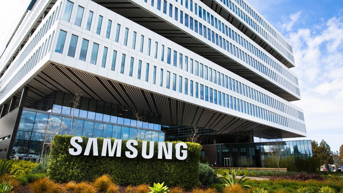
Samsung opens next-gen 3D DRAM research lab in the United States
Samsung's latest research lab operates under "Device Solutions America," is based in Silicon Valley
Samsung is currently in the process of developing next-gen 3D DRAM on American soil, says The Korea Times, according to its own industry sources. The lab for this next-gen 3D DRAM development is based in Silicon Valley, operating under the "Device Solutions America" division, or DSA for short.
Apparently, the goal of this lab is to develop an upgraded DRAM model that will allow Samsung to take leadership of the global 3D DRAM market— that's, again, according to Korea Times' reporting on the matter.
For those unfamiliar, "3D DRAM" refers to DRAM being manufactured with a "3D" process. The goal of 3D manufacturing processes is to make better use of physical hardware restraints by "stacking" dies, memory modules, etc on top of each other. Over in the world of CPUs, for example, we have something called "3D Cache", which refers to regular CPU L3 cache that's "stacked" in manufacturing to improve onboard memory capacity. And of course, Samsung pioneered 3D stacked NAND (Samsing calls it V-NAND) for SSD storage more than a decade ago.
As the benefits of 3D cache on desktop CPUs have already demonstrated themselves, Samsung's comments on the improvements offered by 3D DRAM seem quite promising. Korea Times reports a Samsung comment made in October 2023, where they claimed that new structures for sub-10nm DRAM will allow for larger single-chip capacities that can exceed 100 gigabits.
In short, Samsung's work on 3D DRAM could very much be pushing the envelope forward in terms of memory capacity. 3D stacking in CPU manufacturing for increased L3 cache is already proven to work as a method of dramatically boosting capacity, and performance in that constrained workload.
While most modern consumer PCs are hardly hurting for more DRAM, Samsung continuing to push the envelope forward should prove beneficial to the computing market at large. Server operators and the highest-end enthusiasts would benefit first, but normalizing 3D DRAM should serve to both boost the high-end of RAM capacities and lower the cost for the entry-level, as most major advances in PC hardware do.
Time will tell just how successful and dominant Samsung's 3D DRAM will become, though, and exactly how long we'll have to wait for these solutions to become available. For now, we'll just have to be satisfied in know Samsung's Silicon Valley lab is working to push the apparent next generation of DRAM manufacturing forward.

