Array
(
    [content] => 
    [params] => Array
        (
            [0] => /forum/index.php?threads/first-euv-light-marks-key-milestone-for-production-of-intel-4-in-europe.17258/
        )

    [addOns] => Array
        (
            [DL6/MLTP] => 13
            [Hampel/TimeZoneDebug] => 1000070
            [SV/ChangePostDate] => 2010200
            [SemiWiki/Newsletter] => 1000010
            [SemiWiki/WPMenu] => 1000010
            [SemiWiki/XPressExtend] => 1000010
            [ThemeHouse/XLink] => 1000970
            [ThemeHouse/XPress] => 1010570
            [XF] => 2021370
            [XFI] => 1050270
        )

    [wordpress] => /var/www/html
)

First EUV light marks key milestone for production of Intel 4 in Europe

Daniel Nenni

Admin
Staff member
Intel’s first European high volume EUV scanner, located at its Fab 34 facility in Ireland, generated its 13.5 nanometre wavelength light for the first time this week.

December 22, 2022

Earlier this year Fab 34 in Ireland took delivery of its first EUV lithography system, a key enabler of Intel 4 process technology. The system, made by Dutch manufacturer ASML, is arguably the most complicated piece of machinery humans have ever built. Since its arrival, local teams have been working through the installation phase and this week reached an important moment as the EUV scanner generated its 13.5 nanometre wavelength light for the first time in Ireland.

This is a key milestone on the path towards high volume production of Intel 4 technology and is the first time a high volume EUV scanner will be used in Europe.

Preparing for a critical milestone
The EUV system consists of 100,000 parts, 3,000 cables, 40,000 bolts and more than a mile of hosing. It took 18 months of design and construction activity to prepare the Fab 34 building to receive the machine. Following its arrival in Leixlip, the journey to generating first light has been an incredibly complex one that relied upon the intricate alignment of multiple factors. From the build of the scanner itself to the qualification of facility systems and the connection to utilities, it has taken a huge, combined team effort to reach this point.

Generating first light
In the lithography process, patterns are transferred to a silicon wafer, creating the blueprints for our integrated circuits. While lithography scanners have been an integral part of making microchips for many years, EUV scanners can print circuitry smaller and more precisely than anything that has come before.

The systems to support the EUV scanner begin at the utility, or basement, level of the fab where the vacuum pumps to create the vacuum environment and RF control cabinets for power inputs to the laser, are located.

In the Subfab – which is located directly below the cleanroom - we have a powerful 25KW laser that generates light fired at 50,000 times per second as well as a suite of control and purification cabinets. This laser light travels up through a beam transport system to the EUV tool which is located in the main fab cleanroom.
Inside the tool, molten tin droplets are fired and struck twice by the laser. The first low power strike turns the tin droplet into a pancake shape. The second high energy strike creates the EUV plasma to form the 13.5 nanometre light which is reflected through mirrors to pick up the design template – called a reticle - and pattern it to the silicon wafer. This week, the light was produced for the very first time in our first high volume EUV scanner in Europe.

Intel 4 process technology
This milestone has been many years in the making. The planning, preparation and precision required to deliver EUV lithography in high volume production is unparalleled. The arrival of this important moment ushers the way for Intel 4 technology, which has achieved its key milestone of manufacturing readiness by 2H 2022 for products such as Meteor Lake in 2023. Intel's unique process innovations and approach to EUV with the Intel 4 process keep Intel on track to deliver five nodes in four years and meet its commitment to regain process leadership by 2025.

Over 100 ASML staff are supporting the build and set up of the system together with teams of trade contractors, Intel Engineers and Technicians.
In addition, a number of people from the local Intel team have spent time on seed assignment at our technology development fab in Oregon in order to ensure that Fab 34 was ready for this awesome technology.

Fab 34 is excited to take one step closer to running wafers and delivering products to our customers.


newsroom-ire-2022-euv-first-light-5.jpg.rendition.intel.web.1648.927.jpg

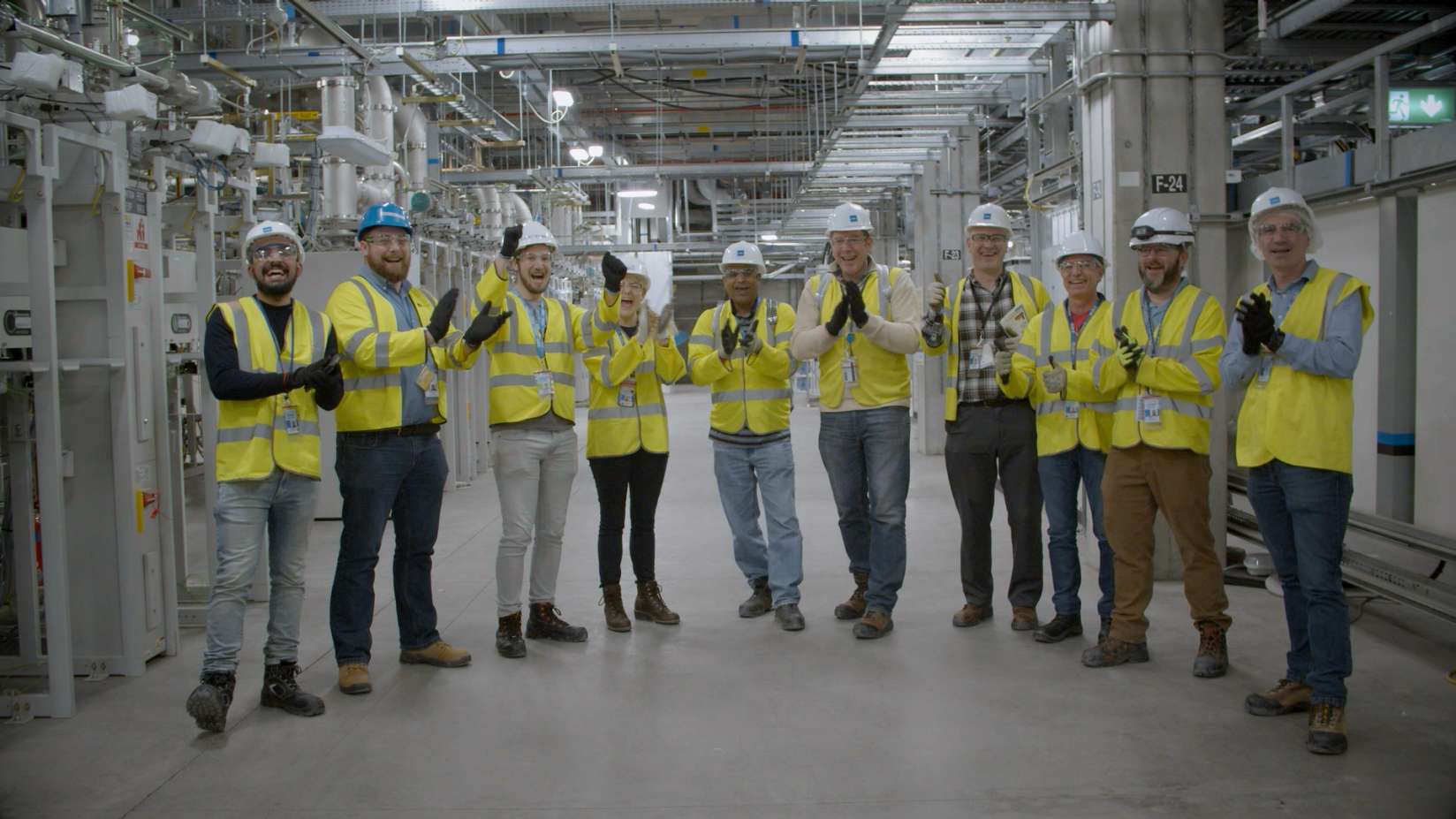
It has taken a huge, combined team effort to deliver this milestone (credit: Intel Corporation)
newsroom-ire-2022-euv-first-light-6.jpg.rendition.intel.web.1648.927.jpg

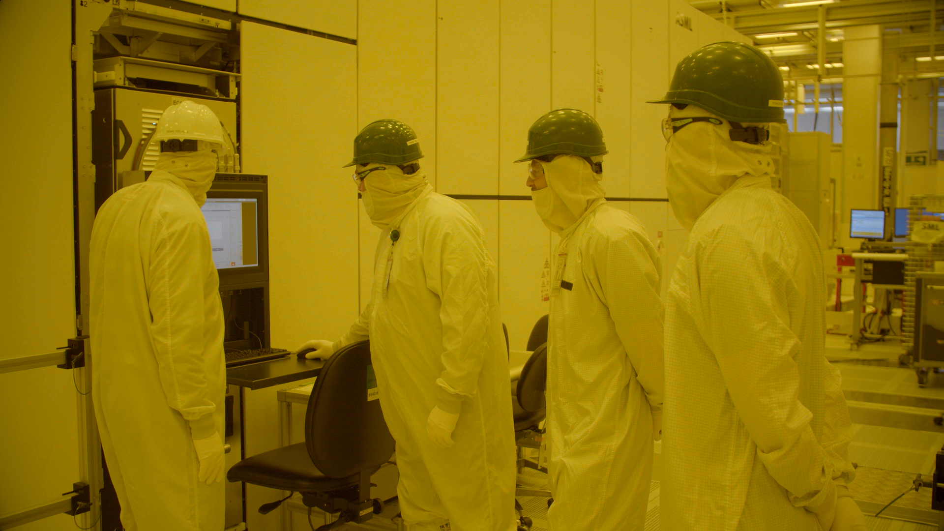
ASML staff are supporting the EUV system set up together with teams of trade contractors and Intel employees (credit: Intel Corporation)
newsroom-ire-2022-euv-first-light-1.jpg.rendition.intel.web.1648.927.jpg

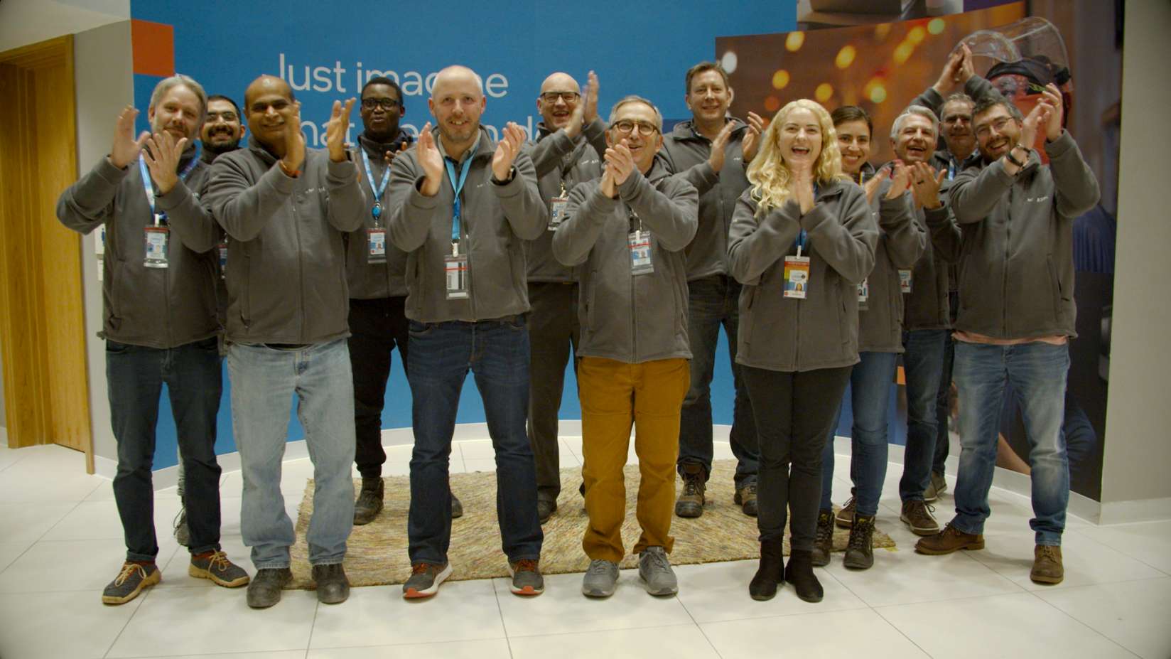
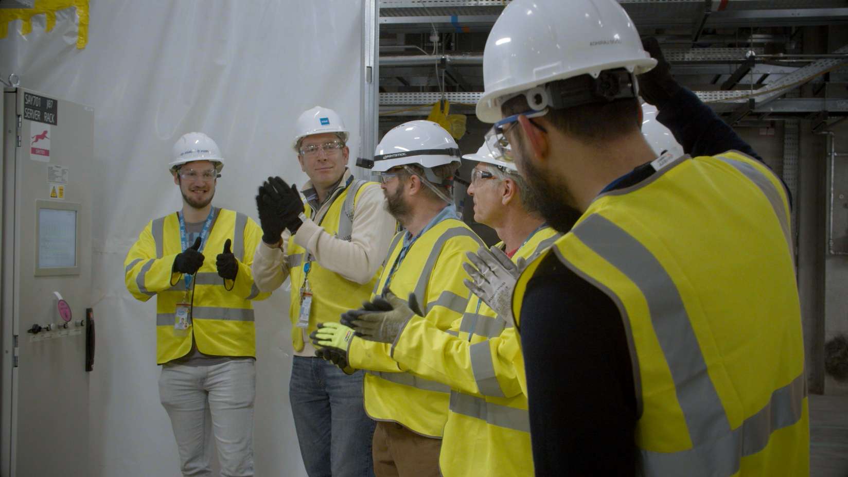
Teams working at the Fab 34 utility level celebrate the first EUV light in Ireland (credit: Intel Corporation)
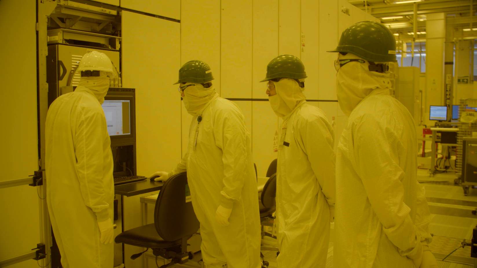
newsroom-ire-2022-euv-first-light-2.jpg.rendition.intel.web.1648.927.jpg

The EUV scanner generated its 13.5 nanometre wavelength light for the first time in Ireland (credit: Intel Corporation)
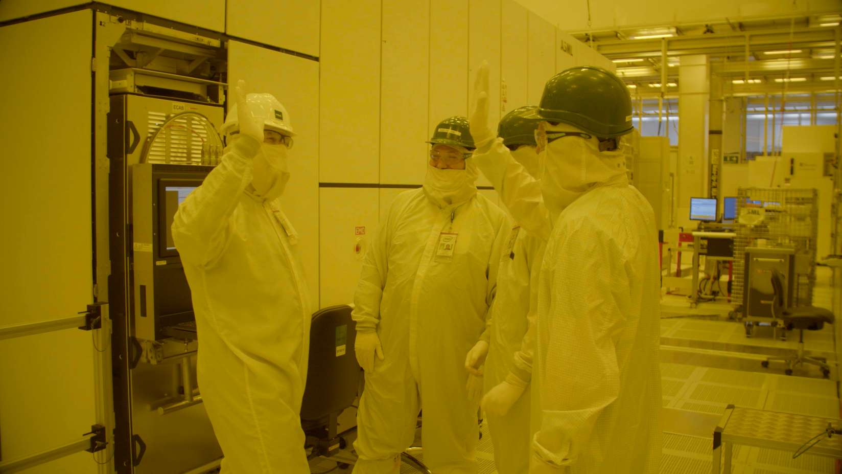
newsroom-ire-2022-euv-first-light-3.jpg.rendition.intel.web.1648.927.jpg

The EUV system is made by Dutch manufacturer ASML (credit: Intel Corporation)
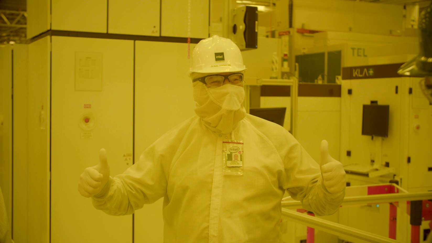
newsroom-ire-2022-euv-first-light-4.jpg.rendition.intel.web.1648.927.jpg

Intel's Donal Coghlan celebrates the important milestone (credit: Intel Corporation)
It has taken a huge, combined team effort to deliver this milestone (credit: Intel Corporation)
ASML staff are supporting the EUV system set up together with teams of trade contractors and Intel employees (credit: Intel Corporation)
Teams working at the Fab 34 utility level celebrate the first EUV light in Ireland (credit: Intel Corporation)
The EUV scanner generated its 13.5 nanometre wavelength light for the first time in Ireland (credit: Intel Corporation)
 
It will be a good case study about why Intel is more than three to four years behind TSMC on using EUV in high volume production. Intel was once the largest corporate investor who invested in ASML.
 
It will be a good case study about why Intel is more than three to four years behind TSMC on using EUV in high volume production. Intel was once the largest corporate investor who invested in ASML.
Not necessarily. D1 has been using a large number of EUV tools for a while now. Just on a quick google map search D1 also appears to have more cleanroom space than Ireland (especially when one considers that Ireland also needs to continue making legacy processes). The former 7nm was so heavily delayed at this point that I would have to assume they have worked out many of the worst issues. Combine this with maintenance and many operations tasks being managed by ASML staff, and I am guessing that Intel is more like 2 years behind TSMC in EUV experience. For me it is hard to believe that across the like 3 years of delays and year of risk starts that Intel’s EUV competence is worse than TSMC in the 7nm era when one considers that N7+ was just one layer. Intel is further aided by intel 4/3 not making extensive use of EUV multi patterning.

The wider world will get a better picture during the second half of 2023 when we can see how many new laptops are using meteorlake. Of course we won’t know what the theoretical tool capabilities are at D1, but if Intel is really more than 4-5 years behind in EUV expertise then we would most definitely see it reflected in meteorlake stock.

I'm talking about utilizing EUV in high volume manufacturing (HVM). TSMC started HVM using EUV on its N7+ process in Q2 2019 while Intel will start using EUV in HVM sometime in 2023 (best scenario, I guess).

That's 3 to 4 years behind in terms of HVM.

Intel had the money, engineers, capability, and connections to acquire EUV tools but chose not to do it. Now it's doing a catch-up game.
Bigger question to me is why Samsung didn't buy more? It poses as the biggest or leading EUV enthusiast.
 
Is there any realistic scenario when Samsung can seriously challenge TSMC again? It seems they are weakening at exactly wrong the time, as simultaneously TSMC is hitting a real inflection point. The memory business is taking a beating just as TSMC is accelerating away. I just can't find a sequence of events where they can seriously threaten TSMC again going forward. I welcome anyone poking holes in this.
 
Last edited:
I'm talking about utilizing EUV in high volume manufacturing (HVM). TSMC started HVM using EUV on its N7+ process in Q2 2019 while Intel will start using EUV in HVM sometime in 2023 (best scenario, I guess).

That's 3 to 4 years behind in terms of HVM.
I am aware. But my point was that intel has at this point made a large number of EUV wafers and had their EUV tools for a long time. I would have to imagine years of low-med volume are much better than 0 years of experience, and in my opinion is similar to a year of only adding EUV to one layer. Intel also has the benefit of the ASML engineers having seen/fixed many of the early teething issues. I am not saying that there is no gap. Rather that I would think that intel and their suppliers have had enough time and experience that the issues we saw with 7LPP should not be present for intel in 2023. Intel likely already went through the worst of them in 2020-22.

Intel had the money, engineers, capability, and connections to acquire EUV tools but chose not to do it. Now it's doing a catch-up game.
Too much hindsight in this statement for my liking. When 10nm was originally due EUV was years away from being used for one singular layer by TSMC. By the time that it did come out it was ready, it was too late to justify rearchitecting the whole program to take advantage. You might say that they should have had the foresight to do the N7 thing of designing it to be insertble. However that doesn't really hold up super well given that intel was supposed to move to 7nm by 2019 and intel's business model not seeing any benefit to making a 10nm EUV version. As we all know these were bad bets/assumptions and TSMC hit the goldilocks zone for EUV (not too conservative like intel and not too aggressive like Samsung), but this was not exactly obvious in 2014 (nor would the big three know exactly what the other's plans were).
 
Is there any realistic scenario when Samsung can seriously challenge TSMC again? It seems they are weakening at exactly wrong time as simultaneously TSMC is hitting a real inflection point. The memory business is taking a beating just as TSMC is accelerating away. I just can't find a sequence of events where they can seriously threaten TSMC again going forward. I welcome anyone poking holes in this.
I fear the same thing. However never count Samsung out. It seems like they do their best work when the chips are down. Look no further than the excellent 14nm coming out well before N16 after their disaster trying to get gate first to yield. They lost their one customer Apple, but with 14nm they got them back (as well as licensing it out to GF). Time is ticking though. Memory downturn, new DRAM and NAND nodes floundering, the China debacle putting a large share of their capacity at risk, and IFS potentially snagging many of their foundry customers. If Samsung is going to get back on track their gambit of axing their next generation DRAM to try and leapfrog Micron/SK has to work, and 3GAP and beyond need to have some value proposition.
 
I fear the same thing. However never count Samsung out. It seems like they do their best work when the chips are down. Look no further than the excellent 14nm coming out well before N16 after their disaster trying to get gate first to yield. They lost their one customer Apple, but with 14nm they got them back (as well as licensing it out to GF). Time is ticking though. Memory downturn, new DRAM and NAND nodes floundering, the China debacle putting a large share of their capacity at risk, and IFS potentially snagging many of their foundry customers. If Samsung is going to get back on track their gambit of axing their next generation DRAM to try and leapfrog Micron/SK has to work, and 3GAP and beyond need to have some value proposition.
This is my thesis as well. The memory business is seriously cut throat and it is not going to get any less competitive. From what I have gathered Micron for the time being hold a technology edge over Samsung while at the same time Chinese memory manufactures pose a real threat of flooding the market and are even making progress moving up the value chain. My understanding is the memory business really bankrolls Samsungs logic side of the semi business, so if there position weakens as I expect it do, there they are in strategic bind. If N3 and N3E etc beat Samsung GAA 3nm by an appreciable margin in performance and yield, they are in serious serious trouble. To that end, does anyone know how Samsung 3nm is yielding and performing? By the amount of customers designing for the TSMC N3E, N3P, N3EX etc family there must be clear benefits despite whatever discounts Samsung is giving on 3nm GAA to get back business as I am sure must be offering them left, right and center to get back the likes Tesla, Nvidia, Qualcomm etc. Samsung foundry has lost an astounding amount of very important customers in the last couple years. Its crazy.
 
Bigger question to me is why Samsung didn't buy more? It poses as the biggest or leading EUV enthusiast.
Do they really need more at this moment. Their EUV DRAM has terrible yields, and "4nm" is just a slightly shrunk 7nm with SDB. I can't imagine that they need nearly as many EUV tools for that family of nodes as TSMC needs for N7+, N5 family, and N3.
 
Is there any realistic scenario when Samsung can seriously challenge TSMC again? It seems they are weakening at exactly wrong the time, as simultaneously TSMC is hitting a real inflection point. The memory business is taking a beating just as TSMC is accelerating away. I just can't find a sequence of events where they can seriously threaten TSMC again going forward. I welcome anyone poking holes in this.

I highly doubt it.

EUV is another example of why TSMC will remain the undisputed foundry leader. The shear volume of customers and partners that make up the TSMC ecosystem really is a force of nature. TSMC was late to FinFETS but dominated it at the end with N6/5/4/3. TSMC will be late again to GAA (my opinion) but will come out ahead given time (Déjà vu FinFETs).

Bottom line: TSMC makes decisions based on customer input. Intel and Samsung make decisions based on Intel and Samsung input. Ego is a factor with Intel and Samsung decisions as well. If big HVM customers are not ready to design to GAA them TSMC will wait until they are, absolutely.
Bonus round for you Dan:

1) Does a foundry need to have the same volume and customer breadth as TSMC to be considered a "success" or "viable competitor"? Or would you say that something like Samsung in the 14nm era was a "viable competitor", even if their customer pool was smaller than TSMC.

2) Is there any amount of success on the technological front that can lead to a sufficiently healthy ecosystem? Samsung is technically going to be the first to HNS, with TSMC likely being the last member of the big three to reach HVM. Assuming intel and Samsung put their money where there mouth is and don't choke and fall behind TSMC soon thereafter (not guaranteed but roll with me here), is it possible for one or both of these foundries to attract enough customers to be profitable? Or do you think that it doesn't matter how far behind TSMC is, they will always have the entirety of everybody (minus Qualcomm and trailing edge MediaTek/NVIDIA)'s business?

3) While I highly doubt the following scenario is even possible; what if in 10 years we see an intel or a Samsung consistently have a lead that is similar to what intel experienced during the 2000s thru mid 2010s. Even in this fantasy land scenario I don't see TSMC losing all of their customers. But would the foundry that did do this see a massive surge in popularity? Looking back a few years even the mighty Apple put aside their blood feud/IP theft concerns with Samsung when N16 was late. While I doubt Apple would change sides for say 18A or 2GAE even if they did exactly what was advertised and came out well before N2. Would this be the case if the IDMs were on 10A or 1.0GAE while TSMC only had N1.4? What about people who don't get the same VIP treatment as Apple? In this hypothetical situation I doubt the IDMs would burry TSMC, but it is also hard to believe that the current market shares would stay unchanged.

I guess I ask this because I wonder if there is even a point? Does better technology even matter? Does investing in a foundry ecosystem matter? Is the best course of action for these IDMs to make the best node for their product, and throw out their PDKs in case a Qualcomm wants to help amortize your costs by playing chicken with TSMC? Are SFS and IFS just wastes of time/distractions that could be better spent being fast followers or innovators for the things that matter to their own logic product stacks?
 
Last edited:
Bonus round for you Dan:

1) Does a foundry need to have the same volume and customer breadth as TSMC to be considered a "success" or "viable competitor"? Or would you say that something like Samsung in the 14nm era was a "viable competitor", even if their customer pool was smaller than TSMC.

2) Is there any amount of success on the technological front that can lead to a sufficiently healthy ecosystem? Samsung is technically going to be the first to HNS, with TSMC likely being the last member of the big three to reach HVM. Assuming intel and Samsung put their money where there mouth is and don't choke and fall behind TSMC soon thereafter (not guaranteed but roll with me here), is it possible for one or both of these foundries to attract enough customers to be profitable? Or do you think that it doesn't matter how far behind TSMC is, they will always have the entirety of everybody (minus Qualcomm and trailing edge MediaTek/NVIDIA)'s business?

3) While I highly doubt the following scenario is even possible; what if in 10 years we see an intel or a Samsung consistently have a lead that is similar to what intel experienced during the 2000s thru mid 2010s. Even in this fantasy land scenario I don't see TSMC losing all of their customers. But would the foundry that did do this see a massive surge in popularity? Looking back a few years even the mighty Apple put aside their blood feud/IP theft concerns with Samsung when N16 was late. While I doubt Apple would change sides for say 18A or 2GAE even if they did exactly what was advertised and came out well before N2. Would this be the case if the IDMs were on 10A or 1.0GAE while TSMC only had N1.4? What about people who don't get the same VIP treatment as Apple? In this hypothetical situation I doubt the IDMs would burry TSMC, but it is also hard to believe that the current market shares would stay unchanged.

I guess I ask this because I wonder if there is even a point? Does better technology even matter? Does investing in a foundry ecosystem matter? Is the best course of action for these IDMs to make the best node for their product, and throw out their PDKs in case a Qualcomm wants to help amortize your costs by playing chicken with TSMC? Are SFS and IFS just wastes of time/distractions that could be better spent being fast followers or innovators for the things that matter to their own logic product stacks?
I know the question isn't aimed at me but I found this an interesting thought experiment about if tech lead really matters when an ecosystem is so superior. I actually don't know and would be lying if I said I did.
 
Last edited:
I am aware. But my point was that intel has at this point made a large number of EUV wafers and had their EUV tools for a long time. I would have to imagine years of low-med volume are much better than 0 years of experience, and in my opinion is similar to a year of only adding EUV to one layer. Intel also has the benefit of the ASML engineers having seen/fixed many of the early teething issues. I am not saying that there is no gap. Rather that I would think that intel and their suppliers have had enough time and experience that the issues we saw with 7LPP should not be present for intel in 2023. Intel likely already went through the worst of them in 2020-22.


Too much hindsight in this statement for my liking. When 10nm was originally due EUV was years away from being used for one singular layer by TSMC. By the time that it did come out it was ready, it was too late to justify rearchitecting the whole program to take advantage. You might say that they should have had the foresight to do the N7 thing of designing it to be insertble. However that doesn't really hold up super well given that intel was supposed to move to 7nm by 2019 and intel's business model not seeing any benefit to making a 10nm EUV version. As we all know these were bad bets/assumptions and TSMC hit the goldilocks zone for EUV (not too conservative like intel and not too aggressive like Samsung), but this was not exactly obvious in 2014 (nor would the big three know exactly what the other's plans were).

Like what you pointed out there are several good reasons why Intel is late in adopting EUV. IMO, two additional factors must be considered:

1. Intel put wrong attention to its short term stock price. Huge and precious cash was pumped into dividends and stock buyback. The stock buyback program especially was a suicidal program that's strangling Intel.

Here was what I said on February 22, 2022:

"Intel's market capitalization is at $181.93 billion today. Compare this $181.93 billion market cap to $67.9 billion (stock buyback spending since 2012) or $102.8 billion (stock buyback spending since 2005), isn't it ridiculous?"

As of 12/23/2022, intel's market capitalization has dropped further to $107.67 billion.

Source: Post in thread 'Intel Investor Meeting Keynote' https://semiwiki.com/forum/index.php?threads/intel-investor-meeting-keynote.15543/post-51014

2. Intel placed too many nice but unfit persons into its senior leadership team and Board of Directors. Many bad decisions, such as stock buyback program and EUV strategy, can be traced back to it.

Now Intel recognized it and started fixing it. But the damage had been done.
 
Last edited:
Back
Top