Great read but I think 2021 is a bit optimistic:
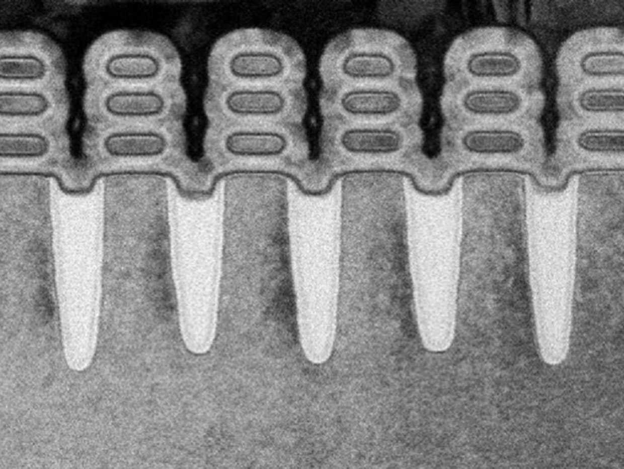
The Shape of Things to Come: Nanosheet field-effect transistors flow current through multiple stacks of silicon that are completely surrounded by the transistor gate. The design reduces avenues for current to leak through and boosts the amount of current the device can drive.

Snip......
The FinFET has no doubt been a great success. Though it was invented more than a decade earlier, the FinFET was first commercially introduced in 2011 at the 22-nm node by Intel and later by Samsung, TSMC, and others. Since then it’s been the workhorse of cutting-edge silicon logic in these final stages of Moore’s Law scaling. But all good things come to an end.
With the 3-nm node, FinFETs are not up to the task. The three of us saw this coming in one form or another more than a decade ago, as did others.
Excellent as it is, the FinFET has its problems. For one, it introduced a design limitation that wasn’t a factor for the old “planar” transistor. To see the problem, you have to understand that there’s always a trade-off among a transistor’s speed, power consumption, manufacturing complexity, and cost. And that trade-off has a lot to do with the width of the channel, which is called Weff in device-design circles. More width means you can drive more current and switch a transistor on and off faster. But it also requires a more complicated, costly manufacturing process.
In a planar device, you can make this trade-off simply by adjusting the geometry of the channel. But fins don’t allow as much flexibility. The metal interconnects that link transistors to form circuits are built in layers above the transistors themselves. Because of this, the transistor fins can’t really vary very much in height—equivalent to width in planar designs—without interfering with the interconnect layers. Today, chip designers get around this problem by making individual transistors that have multiple fins.
Another of the FinFET’s shortcomings is that its gate surrounds the rectangular silicon fin on only three sides, leaving the bottom side connected to the body of the silicon. This allows some leakage current to flow when the transistor is off. Many researchers reasoned that to gain ultimate control over the channel region, the gate needed to surround it completely.

 spectrum.ieee.org
The Shape of Things to Come: Nanosheet field-effect transistors flow current through multiple stacks of silicon that are completely surrounded by the transistor gate. The design reduces avenues for current to leak through and boosts the amount of current the device can drive.
Snip......
The FinFET has no doubt been a great success. Though it was invented more than a decade earlier, the FinFET was first commercially introduced in 2011 at the 22-nm node by Intel and later by Samsung, TSMC, and others. Since then it’s been the workhorse of cutting-edge silicon logic in these final stages of Moore’s Law scaling. But all good things come to an end.
With the 3-nm node, FinFETs are not up to the task. The three of us saw this coming in one form or another more than a decade ago, as did others.
Excellent as it is, the FinFET has its problems. For one, it introduced a design limitation that wasn’t a factor for the old “planar” transistor. To see the problem, you have to understand that there’s always a trade-off among a transistor’s speed, power consumption, manufacturing complexity, and cost. And that trade-off has a lot to do with the width of the channel, which is called Weff in device-design circles. More width means you can drive more current and switch a transistor on and off faster. But it also requires a more complicated, costly manufacturing process.
In a planar device, you can make this trade-off simply by adjusting the geometry of the channel. But fins don’t allow as much flexibility. The metal interconnects that link transistors to form circuits are built in layers above the transistors themselves. Because of this, the transistor fins can’t really vary very much in height—equivalent to width in planar designs—without interfering with the interconnect layers. Today, chip designers get around this problem by making individual transistors that have multiple fins.
Another of the FinFET’s shortcomings is that its gate surrounds the rectangular silicon fin on only three sides, leaving the bottom side connected to the body of the silicon. This allows some leakage current to flow when the transistor is off. Many researchers reasoned that to gain ultimate control over the channel region, the gate needed to surround it completely.

The Nanosheet Transistor Is the Next (and Maybe Last) Step in Moore’s Law
Nanosheet devices are scheduled for the 3-nanometer node as soon as 2021
 spectrum.ieee.org

