
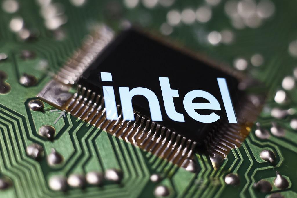
Intel has only recently moved to expand its domestic fabrication operations to a globally competitive scale, largely in response to expected CHIPS Act funding.
With Congress hurtling toward an end-of-week deadline to avert a partial government shutdown, lawmakers are racing to pass appropriations to keep the government open. The House passed its “minibus” legislation containing half of fiscal year 2024’s appropriations Wednesday, and the Senate is set to follow suit today. Another minibus is expected by March 22, the second partial shutdown deadline.
The rushed appropriations package, which was only released last Sunday night, has led to a familiar scenario on Capitol Hill: lawmakers rushing to review and vote on hundreds of pages of bill text riddled with obscure and often unexpected provisions. The scramble has created an opportunity for committee heads and appropriators to stash a number of controversial policies in the legislation. One such provision would slash a fifth of the funding for the Department of Justice’s Antitrust Division as the agency prepares to take on several major cases in the coming year.
But the cut to antitrust enforcement is not the only threat the appropriations package poses to President Biden’s pro-competition agenda. The package also includes $3.5 billion over three years for microchip giant Intel to create a “secure enclave” facility that would exclusively produce highly sensitive microchips for the U.S. military. Instead of providing new funding for the facility, the bill pulls the money from the $39 billion allocated for manufacturing grants by the 2022 CHIPS and Science Act (commonly referred to as the CHIPS Act). Experts and congressional sources say the move threatens to further strain a fund that is already much too small to meet the needs of U.S. semiconductor manufacturers.
“My first reaction is to emphasize that this is nearly 10 percent of the entire CHIPS Act fund,” Charles Wessner, a senior adviser at the Center for Strategic and International Studies and research professor at Georgetown University. “And by doing this, that will necessarily foreclose other opportunities.”
While the United States has several leading chip design companies—Intel first and foremost—the CHIPS Act’s primary purpose was to provide funding to onshore the actual fabrication of microchips, a part of the industry that is currently dominated by Taiwan’s TSMC and South Korea’s Samsung. (Both companies are angling for their own slice of the grant funds to expand their operations in the United States; TSMC is building a fab in Arizona.) Intel has only recently moved to expand its domestic fabrication operations to a globally competitive scale, largely in response to expected CHIPS Act funding.
Instead of providing new funding for the facility, the bill pulls the money from the $39 billion allocated for manufacturing grants by the 2022 CHIPS and Science Act.
The Department of Commerce, which oversees the funds, has begun slowly rolling out its initial awards to domestic chip manufacturers, naming BAE Systems, Microchip Technology, and GlobalFoundries as its first three confirmed awardees. Despite reports indicating Intel is set to receive the lion’s share of the available funding with a package worth over $10 billion, the corporation is reportedly still in tough negotiations with the Department of Commerce for more. In a sign the company is playing hardball, it indicated last month that it plans to slow its expansion of its Ohio manufacturing plant, citing dissatisfaction with the rollout of CHIPS funds as part of its reasoning. If Intel’s package expands any further, it is unlikely the department will be able to adequately fund several other promising proposals. Commerce Secretary Gina Raimondo has indicated that the funding requests the department has received are for twice the available funds—with many more expected to continue rolling in.
The secure enclave earmark for Intel in the appropriations package drains that available CHIPS funding even further. And it is far from clear that the facility is a worthwhile investment. Two congressional staffers, who were granted anonymity to speak openly about the jockeying over the funds that the Department of Defense—the sole customer for the chips Intel is set to produce, aside from a tiny amount meant for intelligence agencies—has not requested the creation of a secure enclave facility. In fact, there is reason to believe the Pentagon actively opposes the plan.
One of those congressional aides instead described the funding as a solution in search of a problem. “We have systems for getting the military the sensitive chips it needs,” they said, referring to an accreditation process already in place within the Department of Defense and emerging innovations that make it possible to assess the integrity of a chip at various stages of the production life cycle. “We could be investing more in modernizing technologies we already have to make it easier and more secure for any supplier to build these chips.”
The aide claims the push for a secure enclave facility began in 2021 with a report from U.S. intelligence agencies that described an unknown risk requiring heightened security at the fabrication stage—the stage of chip production the secure enclave method is primarily designed to protect. While the intelligence committees in both chambers are said to have communicated the report’s conclusion to other relevant committees, the justification for its findings has not been widely dispersed, even to members of the House and Senate Armed Services Committees, many of whom only became aware of the secure enclave project provisions mere hours before the appropriations package text was released this weekend.
Representatives of both chambers’ Intelligence Committee chairs, Rep. Mike Turner (R-OH) and Sen. Mark Warner (D-VA), did not respond to a request to comment for this article. (Conspicuously, the top two Republicans on the House Intelligence Committee, Turner and Rep. Brad Wenstrup, both hail from Ohio, where Intel has recently slowed its expansion plans.)
Further complicating matters, the alleged conclusion of the mysterious intelligence report was contradicted by a report on current and emerging chip security models from the Air Force last August, which claimed that fabrication is the stage in the production process where microchips face the lowest security risk. (The secure enclave will potentially bring testing and packaging in-house as well, production stages that are deemed higher-risk.) The report goes on to specifically say “we need to invest less [in fabrication protections],” and claims that the economics of the highly sensitive chip market—which accounts for an estimated 2 percent of the total U.S. semiconductor marketplace—make it so the Department of Defense “cannot maintain dedicated facilities.” It also emphasizes that it is in the department’s “interest to have access to multiple sources of microelectronics components for resiliency and cost competitiveness.”
The congressional aide who highlighted the conflicting reports indicated that, by siphoning such a large portion of the funds meant to boost domestic manufacturing capacity, the mandate to fund the secure enclave project stands to make the goal of diversifying the supply chain for sensitive chips much more difficult. The hefty price tag to maintain the facility over time is also likely to create an incentive structure for the Department of Defense to source as many chips as possible from the facility, so as to justify the expense. The aide suggested the ongoing dispute may have been a factor in why CHIPS grant announcements have been slower to materialize than many observers anticipated.
Siphoning such a large portion of funds meant to boost domestic manufacturing capacity makes diversifying the supply chain for sensitive chips much more difficult.
It is unclear which of the conflicting risk assessments the Department of Commerce finds more credible. The funding for the secure enclave project was set to be approved through Commerce’s grant disbursement process, which would have made specific direction from Congress unnecessary. The report also noted that Sens. Maria Cantwell (D-WA), Roger Wicker (R-MS), and Jack Reed (D-RI) sent a letter to Commerce questioning the Intel facility, on grounds similar to those laid out in the Department of the Air Force’s report. The sudden move by appropriators to mandate funding for the project indicates that Commerce, which has been consulting with the Pentagon in its distribution of grant funds, may have had second thoughts.
It is also unclear if or how the secure enclave funding might impact the grants Commerce has already announced but not finalized for Intel’s competitors BAE Systems and GlobalFoundries, both of which are key parts of the defense microchip supply chain. The Department of Commerce, which did not immediately respond to a request to comment for this article, said it is“still reviewing the effect of the appropriations text on the program.”
The second minibus package, which includes appropriations for defense and like the first is currently taking shape behind closed doors, presents an obvious opportunity for Congress to undo the mandate and return the decision over how to allocate grant money to the Department of Commerce. At the very least, the package could allocate new funds to support the project, or redirect money from other parts of the Pentagon’s hefty budget to backfill the hole it leaves in the CHIPS Act manufacturing grant pot. But if legislators truly want to advance their goals of building out domestic microchip manufacturing capacity, they need to go a step further and expand, not commandeer, the fund.
“Congress is going to learn very quickly that $39 billion isn’t a lot of money in the microchip world,” Wessner said, pointing out that China has spent many multiples of that amount in the last decade. “[The $39 billion] can’t be a one and done. We have to have a regular flow of resources, or we can’t compete. Period.
Intel’s $3.5 Billion Boondoggle
Intel’s ‘secure enclave’ project will take nearly 10 percent of a CHIPS Act manufacturing fund that is already stretched thin.
 www.ic-pcb.com