
Ever sat around waiting for a time slot on the one piece of big, powerful, expensive engineering equipment everyone in the building wants to use? It’s frustrating for engineers, and a project manager’s nightmare: a tool that can deliver big results, and a lot of schedule juggling.
In the arena of FPGA-based prototyping, the industry has created just such a conundrum. The drive for bigger, faster, more complex SoC designs made the objective of a bigger, faster, more complex – and more expensive – FPGA-based prototyping platform desirable. True, one needs to explore any option against its alternatives, and compared to even more expensive emulator platforms and relatively inexpensive but less accurate virtual prototyping tools, there are benefits.
When we last visited with Mick Posner on the Synopsys HAPS-70 platform, we took a bit of a different look at the problem. Bigger is important, because one of the biggest stumbling blocks in SoC design is what happens or doesn’t happen at integration. By having an FPGA-based prototyping platform large enough to hold an entire design, IP blocks are represented in full fidelity and interfacing problems can be exposed and debugged.
Another part of the HAPS-70 story is reusable validation IP, with RTL and timing and scripts and pinouts able to move forward as designs progress to integration. This includes a hybrid prototyping strategy, combining the benefits of a virtual prototype with the HAPS-70 platform by introducing a set of AMBA transactors.
The next part of the story is about what went right. As customers bought into the HAPS-70 platform and found the benefits in successful SoC integration, many of them with bigger design teams ran into the scenario we described in the opening. In order to feed forward IP, IP teams have to be able to use the platform – but if the platform is always tied up with integration of the complete SoC product, they have a hard time getting back on once the design wheel is rolling.
Of course, a firm could buy a second HAPS-70, or a third … but realistically, even the smallest HAPS-70 family members are somewhat overkill for one IP developer. Also, in some ways the big platforms are more than an IP team really needs to develop a functional block, and in other ways they don’t support tasks like detailed debug as easily as they should. As the number of IP blocks in designs is exploding, a firm may have ten or more teams working on blocks simultaneously, each needing their own platform set up for typical IP debug tasks.
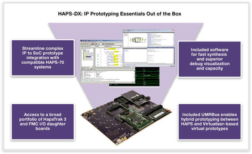
Posner’s team has created the Synopsys HAPS Developer eXpress, or HAPS-DX for short, with the IP team in mind. HAPS-DX targets IP designs around 4 million gates with up to 52 high-speed I/O links, so it doesn’t compromise on performance, and the hardware uses many of the same HAPS-70 constructs scaled to a platform for IP developers.
HAPS-DX goes after a more integrated prototyping experience, including optimized software for synthesis and built-in tools for debug. “Getting a working prototype typically has very little to do with the hardware; it’s all about the software,” said Posner.

Synthesis for prototyping means a strategy for reducing bring-up time, but not losing the ASIC focus of the design effort. HAPS-DX includes a new time-to-first-prototype (TTFP) compiler, with fast synthesis modes, ASIC clock conversion, and a guided design flow leveraging TCL scripting. For IP debug, HAPS-DX also integrates the Deep Trace Debug feature, including 8GB of DDR3 DRAM with the unit, which can capture 128 signals for 5 seconds of data integrated with the Verdi and Siloti visualization tools.
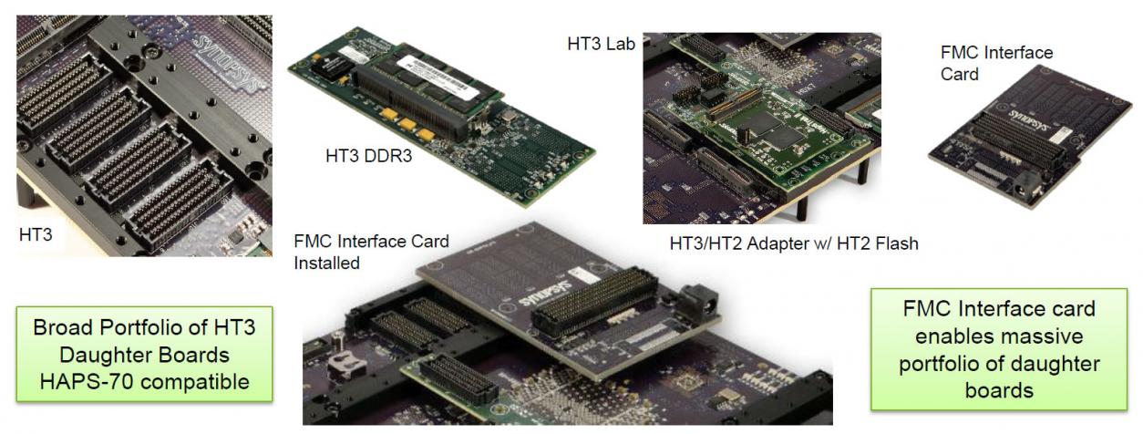
IP is often focused on real-world I/O interfaces, so HAPS-DX brings two daughter board standards: HT3, a smaller Synopsys interface from the HAPS-70 family, and FPGA Mezzanine Card(FMC), an industry standard with hundreds of high-performance daughter cards from numerous vendors.
The hardest customers to satisfy are sometimes internal ones, and Synopsys is no exception: the DesignWare IP teams already use the HAPS-70 platform, and drove the new requirements for the HAPS-DX hard. With a HAPS-DX “on every desk”, IP developers can quickly look at their block with full confidence their work product will feed-forward into the bigger SoC prototyping environment.
While HAPS-70 and its likely successors will continue to grow bigger and more capable for complete SoC designs, HAPS-DX shifts the focus for IP design productivity. Posner has a few items on his 2014 roadmap to help increase productivity for the IP prototyping environment and HAPS-DX even further – stay tuned.
lang: en_US


Comments
0 Replies to “A little FPGA-based prototyping takes the eXpress”
You must register or log in to view/post comments.