With each new silicon process node, the complexity of SoC design rules and physical verification requirements increases significantly. The foundry and an EDA vendor collaborate to provide a “reference flow” – a set of EDA tools and process design kit (PDK) data that have been qualified for the new node. SoC design methodology teams leverage these tool recommendations, when preparing their project plan, confident that the tool and PDK data will work together seamlessly.
The complexity of current package design is increasing dramatically, as well. The heterogeneous integration of multiple die as part of a “System-in-Package” (SiP) module design introduces new challenges to traditional package design methodologies. This has motivated both outsourced assembly and test (OSAT) providers and EDA companies to address how to best enable designers to adopt these package technologies. I was excited to see an announcement from Cadence and Advanced Semiconductor Engineering, or ASE, for the availability of a reference flow and design kit for SiP designs.
I recently had the opportunity to chat with John Park, Product Management Director, IC Packaging and Cross-Platform Solutions, at Cadence, about this announcement and the collaboration with ASE.
In preparation for our discussion, I tried to study up on some of the recent technical advances at ASE.
ASE SiP (and FOCoS) Technology
There is a growing market for advanced SiP offerings, spanning the mobile/consumer markets to very high-end compute applications. The corresponding packaging technology requirements share these characteristics:
- integration of multiple, heterogeneous die (and passives) in complex 2.5D and 3D configurations
- very high chip I/O count and package pin count
- high-density and high-performance signal interconnections between die
- compatibility with high volume manufacturing throughput
- compatibility with thermal management packaging options for high-performance applications (e.g., attachment of thermal interface material (TIM) and a heat sink)
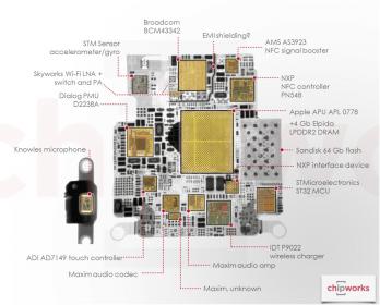
Traditionally, multi-chip modules have used sputtered thin film metallization on ceramic substrates or traces on laminate substrates for signal interconnects – e.g., 10-25um L/S traces are achievable. These SiP packages can be extremely complex, as illustrated below for a smart watch assembly.


Figure 1. SiP for smart watch – top view and cross-section. (From: Dick James, Chipworks, “Apple Watch and ASE Start New Era in SiP”.)
This package incorporates a laminate substrate with underfill, molding encapsulation, and EMI shielding, necessitating intricate Design for Assembly (DFA) rules.
Other SiP applications require high interconnect density between die and high SiP pin counts, as mentioned above – these requirements have necessitated a transition to the use of lithography and metal/dielectric deposition and patterning based on wafer level technology – e.g., < 2-3um L/S redistribution layers (RDL). The volume manufacturing (i.e., cost) requirement has driven development of a wafer-based, bump-attach technology for SiP.
The general class of these newer packages is denoted as fan-out wafer-level processing (FOWLP). ASE has developed a unique offering for high-performance SiP designs – Fan-Out Chip-on-Substrate (FOCoS).

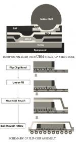
Figure 2. Cross-section and assembly flow for ASE’s advanced SiP, FOCoS. (From: Lin, et al., “Advanced System in Package with Fan-out Chip on Substrate”, Int’l. Conference on Microsystems, Packaging, Assembly and Circuits Technology, 2015.)
The multiple die in the SiP are mounted face-down on an adhesive carrier, and presented to a unique molding process. The molding compound fills the volume between the dice – a replacement 300mm “wafer” of die and compound results, after the carrier is removed. RDL connectivity layers are patterned, underbump metal (UBM) is added, and solder balls are deposited. The multi-die configuration is then flip-chip bonded to a carrier, followed by underfill and TIM plus heat sink attach.
SiP-intelligent design
With that background, John provided additional insight on the Cadence-ASE collaboration.
“SiP technology leverages IC-based processing for RDL fabrication. Existing package design and verification tools needed to be supplanted. Cadence recently enhanced SiP Layout, to provide a 2.5D/3D constraint-driven and rules-driven layout platform. Batch routing support for the signal density of advanced heterogeneous die integration is required.”, John highlighted.
“To accelerate the learning curve for the transition to SiP design, Cadence and ASE collaborated on the SiP-id capability – System-in-Package-intelligent-design.”
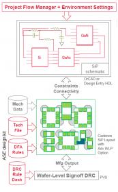
The figure below illustrates the combination of design kit data, tools, and reference flow information encompassed by this partnership.

Figure 3. SiP-id overview. ASE-provided design kit data highlighted inred.
ASE provided the Design for Assembly (DFA) and DRC rules data, for Cadence SiP Layout and Cadence Physical Verification System (PVS).
Further, there are a couple of key characteristics of SiP-id that are truly focused on design enablement.
- The DFA and DRC rules are used by SiP Layout for real time, interactive design checking (in 2D and 3D).
- ASE provides environment setup and workflow support to SiP designers, for managing the data interfaces to ASE, as illustrated below.
and, very significantly,
- As a result, this is a manufacturing sign-off based flow.
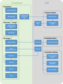
The figures below illustrate the SiP-id customer interface with ASE.


Figure 4. Customer interface with SiP-id.
SiP technology will continue to offer unique PPA (and cost) optimization opportunities, especially for designs integrating heterogeneous die. The collaboration with ASE and Cadence to provide assembly and verification design kit data and release-to-manufacturing reference flows is a critical enablement. ASE is clearly committed to assisting designers pursue the challenges of SiP integration – perhaps their SiP-id web site says it best:
“It is our intention to offer all ASE customers a set of efficient tools where designers can freely experiment with designs which can go beyond the current packaging limits… This is an ongoing effort by ASE, not only to develop fanout (such as Fan-Out Chip on Substrate, FOCoS), panel fanout, embedded substrates, 2.5D, but also to making design tools more user friendly, up-to-date and efficient.”
This is indeed an exciting time for the packaging technology industry.
For more information on Cadence SiP Layout, please follow this link. For more information on the SiP-id reference flow and customer interface to ASE, please follow this link.
-chipguy
Share this post via:


Comments
There are no comments yet.
You must register or log in to view/post comments.