 I recently had the opportunity to chat with Anirudh Devgan, senior vice president and general manager at Cadence, who leads the Digital and Signoff Group. We discussed recent product development initiatives at Cadence, and talked about future EDA and semiconductor market opportunities. His insights and comments were keen — here are the “Top 10” from our conversation.
(10) Customers require a “full digital flow.”
A few years, ago, Cadence made a critical decision to invest significantly in making their digital chip implementation tools more competitive. “In addition to the best PPA, customers are seeking a full flow from RTL-to-signoff,” Anirudh indicated. “The interdependencies between implementation and analysis are so strong that gluing tools just doesn’t work any longer.”
The result has been the release of new products — e.g., Cadence Quantus QRC Extraction Solution, Tempus Timing Signoff Solution, Voltus IC Power Integrity Solution, Genus Synthesis Solution, Innovus Implementation System, Modus Test Solution. Anirudh quipped, “The ’-US’ in these product names is significant. It reflects the customer and Cadence collaboration that is key to our product development.”
(9) A key factor in the software development effort was that algorithms needed to be re-architected to support distributed computation.“Parallelism is a key requirement.”
Realistically, some tightly coupled algorithms are more difficult to re-architect in this manner. Nevertheless, Cadence is clearly focused on managing model complexity and flow performance.
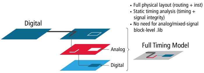
(8) Digital and mixed-signal integration will leverage Cadence’s technology leadership in the analog/custom design space.
As an example, Anirudh highlighted the Cadence Virtuoso mixed-signal timing feature. Digital functionality embedded within an SoC hierarchy — specifically, within a complex analog block — is automatically identified and presented as part of a full timing model to Tempus Timing Signoff Solution for static timing analysis, as depicted in the figure below.

(7) A close collaboration between digital flow developers and the foundry design enablement teams is a must.
No surprise here. Anirudh’s organization is an international one, with developers spanning the globe, and foundry relationship staff in the US, Taiwan, and Korea. The top foundry customers expect reference flows to be available with (early, pre-1.0) PDK releases — that could only happen with a foundry-EDA development partnership.
(6) The cost of production test is a major customer concern.
The latest ‘-US’ product in the Cadence portfolio is “Modus”, an enhanced test insertion architecture used with Genus Synthesis Solution/Innovus Implementation System to provide improved vector compression performance.
SemiWiki’s Pawan Fangaria has written a great article on Modus here.
(5) Cadence is investing significantly in the chip/package/board co-design and analysis space — look for new tools to be introduced.
Then, I asked Anirudh about his view of the broader EDA and semiconductor industry, in general.
(4) There’s plenty of EDA innovation required for complex SoC’s in advanced nodes.
As Mark Twain famously stated, “The reports of my death are greatly exaggerated.” The same applies to those who report the EDA industry is lacking challenges requiring new and innovative approaches.
Anirudh highlighted one area in particular. The need for advancements in routing algorithms in advanced nodes remains very high — not only are performance and power still key optimization objectives, but the lithography requirements are getting more complex with each new node, not to mention the demand for complex mixed-signal circuit routing constraints.
(3) The global semiconductor market is still seeing areas of “explosive growth… the dynamics may change, but there will always be growth.”
Despite predictions of flat of tepid growth in semis, many of the customers Anirudh visits are still experiencing “explosive growth.“ He was extremely optimistic about the opportunities for Cadence flows at new and growing customers, especially because…
(2) “The systems guys want to add semi design capabilities.”
As more system-level companies seek opportunities for product differentiation, they are investing in semi design teams and resources.
Anirudh had a unique perspective on this shift. College engineers studying microelectronics will be encountering a substantially different job market when they graduate. There is a unique “brand value“ in working for a non-traditional system company as a semi engineer.
Which led us to a forward-looking topic on the future of EDA…
(1) The EDA industry, consortia, and government agencies need to invest in EDA-centric research at America‘s universities.
The challenges for design automation are growing, as highlighted earlier. Yet, the sources of the level of funding for academic research that was so strong two decades ago has diminished substantially. As Anirudh succinctly stated, “Collectively, we need to energize the university engine.“
If you get a chance to hear Anirudh speak, or even better, have a one-on-one conversation, you will walk away with additional insights and a better understanding of the dynamics of our industry. I know I did.
-chipguy
Share this post via:


Comments
There are no comments yet.
You must register or log in to view/post comments.