You are currently viewing SemiWiki as a guest which gives you limited access to the site. To view blog comments and experience other SemiWiki features you must be a registered member. Registration is fast, simple, and absolutely free so please,
join our community today!
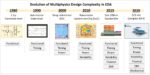
The Electronic Design Automation (EDA) industry used to be a bustling bazaar of scrappy startups, along with medium sized companies that dominated a technology space, and big main-line vendors. The annual Design Automation Conference was noisy, hectic, and sprawled over multiple large convention halls. This diversity meant… Read More
Successful projects leverage the investment in comprehensive methodology and resource planning, covering design and analysis flows – that planning effort is especially important for functional verification.
The emergence of complex SoC designs for advanced automotive applications has led to a major focus on verification… Read More
AIM Photonics held its 2017 Proposers Meetings on May 24[SUP]th[/SUP] in Rochester, NY. The meetings included a review of AIM’s progress and strategic direction by their TRB (technical review board) and a session targeted at PIC (photonic integrated circuit) design for multi-project wafer (MPW) runs. While these discussions… Read More
I had the good fortune to be able to attend a very informative five-day photonic integrated circuit (PIC) training this last week in Santa Clara, CA. The training was organized by Erik Pennings of 7 Pennies consulting and hosted by Tektronix. Several ecosystem partners from the design automation, photonic foundries and photonic… Read More
This week Cadence Design, Lumerical Solutions and PhoeniX Software hosted a two-day photonic summit and workshop. The first day had nearly 100 registered participants and featured industry leaders from Global Foundries, UCSB, MIT, Hewlett Packard Enterprise, General Electric, Boeing, Rockley Photonics, and Juniper Networks… Read More
In August I wrote an article proclaiming Score 1 for IDMs vs Fabless and discussedIntel’sannouncement of volume production of their 100G PSM4 and 100G CWDM4 transceiver products.
This week the Fabless Empire strikes back.Daniel Nenni and I attended a two-day Photonic Summit and workshop hosted by Cadence Design, PhoeniX Software… Read More
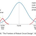
In many ways, static timing analysis (STA) is more of an art than a science. Methodologists are faced with addressing complex phenomena that impact circuit delay — e.g., signal crosstalk, dynamic I*R supply voltage drop, temperature inversion, device aging effects, and especially (correlated and uncorrelated) process… Read More
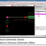
I recently had the opportunity to chat with Anirudh Devgan, senior vice president and general manager at Cadence, who leads the Digital and Signoff Group. We discussed recent product development initiatives at Cadence, and talked about future EDA and semiconductor market opportunities. His insights and comments were keen … Read More
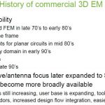
Expanding 3D EM Simulation Access to Allby Tom Dillinger on 02-03-2016 at 7:00 amCategories: Cadence, EDA
James Clerk Maxwell’s eponymous equations are the basis for simulating electromagnetic wave propagation. In school, EE majors tended to fall into two camps: (a) those that thoroughly enjoyed their fields and waves classes, who liked doing surface integrals, and who were adept at demonstrating the “right hand rule”, and (b) … Read More
At the recent TSMC OIP symposium, Bill Acito from Cadence and Chin-her Chien from TSMC provided an insightful presentation on their recent collaboration, to support TSMC’s Integrated FanOut (InFO) packaging solution. The chip and package implementation environments remain quite separate. The issues uncovered in bridging… Read More