This area of automating the design of Flat Panel Displays (FPD) is so broad that it has taken me three blogs to cover all of the details, so in brief review the first two blogs were:
My final blog covers five areas:
- DRC/LVS for curvilinear layout
- Circuit simulation
- RC extraction
- Thermoelectric analysis
- Mask analysis
The following Q&A is with Chen Zhao, from Empyrean, and he’s an AE that’s been with the company since 2014.
Q: IC designers use DRC and LVS tools, so how’s the process different with curvilinear FPDs?
The function of the layout verification tool is to check whether the layout meets the design rules and electrical rules, and whether the layout is consistent with the schematic diagram, etc. 1
It is essential for eliminating errors, reducing design costs and reducing the risk of design failure. General layout verification techniques are developed for rectangular layouts. The emergence of curvilinear-shaped designs poses a great challenge to the layout verification technology. It is necessary to develop new algorithms suitable for curvilinear-shaped designs based on traditional computational geometry algorithms 2, 3.
The grid is used in the layout to determine the position of the graphics, and the vertices of the graphics are on the grid points. The rotation of the layout may cause the vertices and grid points of the graphics to be misaligned, causing the two sides that were originally perpendicular to be no longer perpendicular. Take the next figure as an example. After rotation, “a” and “c”, and “a” and “e” no longer maintain 90 degrees, DRC may report false errors, such as the minimum distance for “a-c” or “d-e” is not enough. At this time, it is necessary to add support angle tolerance rules, by filtering out errors with features such as “small edges” and “small corners” to avoid false errors. Of course, this method has certain risks. The user can output these errors to a specific file to distinguish these minor errors from important errors and check important errors first.
In addition, if you can merge the graphics before rotation, you can also avoid errors.
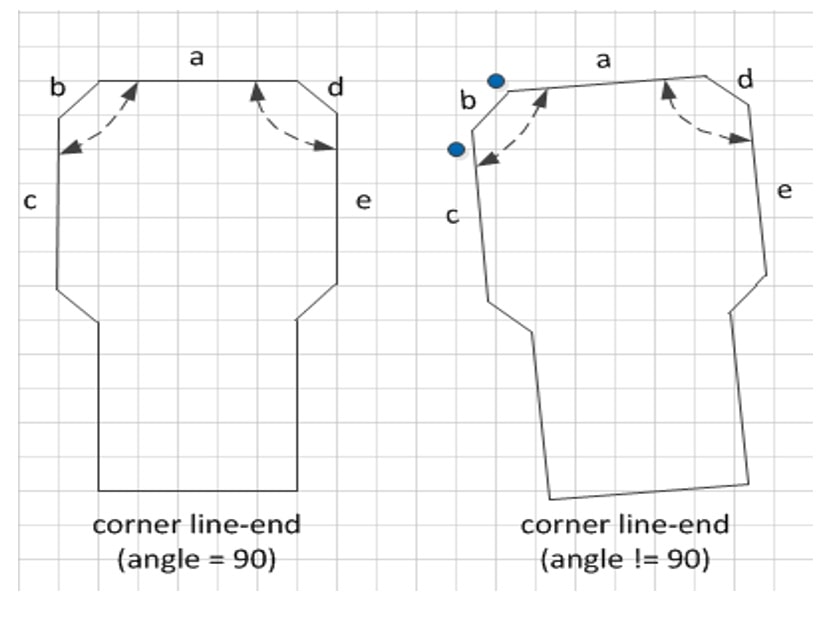
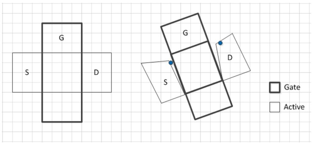
Due to the rotation of the layout, the error increases. LVS may cause the device extraction failure when extracting the circuit netlist.
An MOS transistor example, after rotation, the source and drain terminals do not intersect with the gate due to the dislocation of the vertices and grid points, and the transistor extraction fails. The above DRC methods to eliminate false errors, such as supporting tolerance, merging before graphics rotation, etc., are also applicable to LVS.
ArgusFPD parallel hierarchical layout verification tool developed by Empyrean focuses on the FPD market. It faces the verification needs of ultra-large-scale layouts and advanced design methods such as curvilinear-shaped designs. It provides customers with layout verification solutions that can meet the needs of FPD design sign-off requirements.
Q: How do you simulate large circuits such as an FPD array?
The traditional SPICE simulation of the FPD circuit and the SPICE simulation of the integrated circuit have nothing special except to support the TFT model used in the FPD circuit. As the resolution of the FPD increases, the scale of the FPD circuit becomes larger and larger, and it is unrealistic to use traditional SPICE circuit simulation to achieve a full-panel circuit simulation.
The computational consumption of circuit simulation is mainly divided into two parts, namely SPICE device model calculation and circuit matrix solving 4. For full-panel large circuit simulation, matrix calculation basically occupies more than 90% of the simulation time. Therefore, one way to speed up the circuit simulator is to speed up the matrix solution. Based on this, EMPYREAN’s circuit simulator EsimFPD ALPS developed an adaptive matrix solver 5. It contains a variety of matrix solvers. It can automatically select different matrix solvers, according to different matrix properties (such as dense matrix, sparse matrix, etc.), which can greatly improve the simulation while ensuring the SPICE accuracy of circuit simulation speed
Another method of circuit simulator acceleration is to optimize the simulation algorithm considering the structure of the FPD circuit.
Q: What is the topology of an FPD array?
The structure of the FPD is composed of light-emitting pixel units arranged in a two-dimensional array. As shown below, the cell is the pixel unit. There are three sub-pixels in the cell: red (R), green (G), and blue (B). From the circuit level, the FPD is the top-level circuit, and the cell is the sub-circuit of the next level, and the sub-pixel circuit is the sub-circuit of the next level.
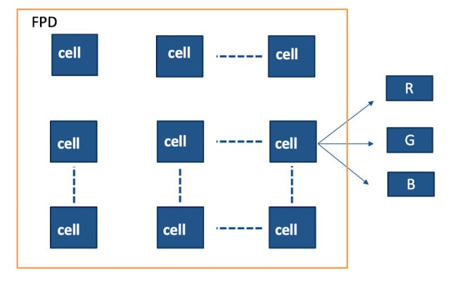
Each cell has the same circuit structure, and each sub-pixel circuit in the cell also has the same circuit structure. These cells have the same circuit structure, and their states are also similar when working, so we can define the cell as a basic unit. The circuit parts with the same structure and the same state only need to store and simulate only one basic unit, and the simulation data is shared with other units, which greatly reduces the simulation time and the required memory.
In addition, using the heterogeneous computing structure of CPU+GPU is a new direction to improve the speed of full-scale circuit simulation 6, 7.
Q: What is your approach for RC extraction to get parasitics into a more accurate netlist for simulation?
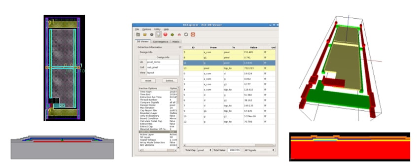
EMPYREAN’s parasitic RC extraction tool RCExplorer FPD provides pixel and touch panel capacitance and resistance simulation analysis tools for a variety of FPD design application scenarios. Based on the parasitic capacitance resistance extraction technology of the accurate three-dimensional field solver, the adaptive meshing technology is adopted to accurately simulate the coupling capacitance.
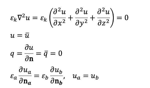
The 3D field solver is based on electric field analysis and uses numerical calculation methods to solve the Laplace equation. The problem of solving capacitance can be transformed into solving the induced charge of a conductor under a certain bias voltage. This problem can be solved by solving the following electromagnetic field equations 8.
The RCExplorer FPD tool also supports pixel-level liquid crystal capacitance extraction, as shown next. At the same time, it can support Gate-on capacitor extraction.
Q: Can you extract a touch panel design layout?
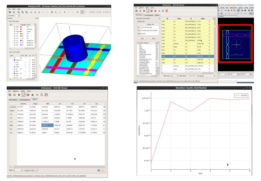
Yes, the RCExplorer FPD can simulate the capacitance of the touch panel in the touch panel design. Due to the large size of the touch panel design and the high requirement for capacitance accuracy, it’s challenging to ensure both high accuracy and performance requirements. The tool uses a meshing method based on following advanced technologies, such as, a mixture of triangle elements and trapezoid elements; intelligent meshing engine automatically determines the degree of density; efficient and adaptive mesh encryption 9, 10; multithreading and multitasking parallel calculations, etc., to ensure the calculation accuracy and calculation speed to meet the design requirements. At the same time, the tool also supports Floating Signal and Finger settings.
With the parasitic capacitance and resistance extracted by RCExplorerFPD, users can perform post-layout analysis to check whether the design load is within an acceptable range, and help designers optimize the layout load design.
Q: How are the thermal-electrical characteristics analyzed for FPD arrays?
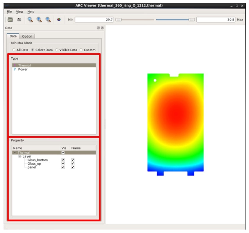
High-precision OLED device current control is extremely important to the uniformity of OLED FPD light emission, and so it is critical to ensure the stability of power and ground potential 11. The EMPYREAN Artemis FPD high-resolution full-panel layout thermoelectric analysis tool analyzes the power/ground voltage drop distribution, current density distribution, and temperature distribution of the FPD, which can effectively help designers optimize the design.
This tool adopts advanced techniques such as accurate resistance calculation method, cascade array netlist output, hierarchical fast calculation method, heat conduction and heat convection, etc., which can quickly and accurately perform full-panel analysis.
The tool uses an array-based accurate resistance calculation acceleration method. The entire flow uses a two-dimensional field solver to calculate the highest precision resistance network, and uses the pixel array hierarchy to quickly calculate the voltage and current distribution of the overall resistance network. It calculates the power and ground potential of each TFT.
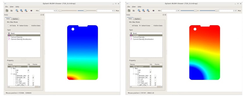
With the wire resistance between the nodes of the resistive network and the voltage across the nodes, together with the device voltage and current information, we can calculate the power value at each node of the entire panel.
With the power distribution, according to the mixed model of heat conduction and heat convection, we can get the heat distribution of the panel.
Q: Why is it important to have Mark Rule Checks (MRC)?
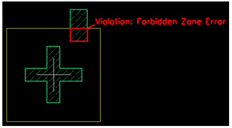
MRC inspection is an important part of the design flow after the mask layout is completed. EMPYREAN’s MRC tool provides the Mask and Glass design engineers with tools to check the correctness of Mark placement. Mark is an important reference for process alignment of exposure, etching and other machines, and has zero tolerance for errors. The MRC tool provides an automated Mark inspection method to improve the reliability of Mark design. It can check more than ten rules and their combinations, such as forbidden zone, symmetry, standard Mark position comparison, and provide clear and easy-to-understand annotation cartoons to mark the location of errors, such as forbidden zone inspection errors.
Q: What are challenges of the largest panel masks?
The Split Panel function provides an FPD design engineer with the function of cutting the panel layout into multiple mask layouts. Split Panel is an essential function in large-size stitching design. When the size of the Panel exceeds the size of the exposure machine, one exposure cannot complete the production of a large-size panel, and it is necessary to stitch the design for multiple exposures to finally complete the production of a panel. Based on the layout of the large-size panel and the size of mask, the Split Panel cuts the panel through guideline or cartoon direct cutting method, thereby dividing it into multiple mask layouts.
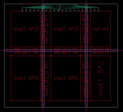
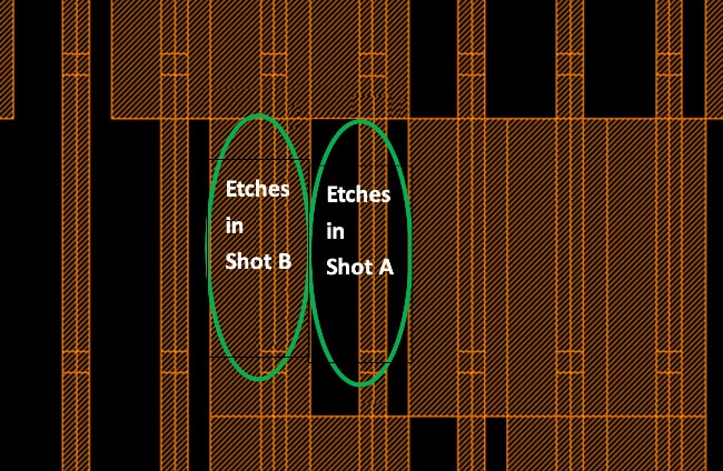
The Split Panel function can automatically call the Mosaic function. If the boundary between two adjacent exposures is a straight cut, the human eye can clearly distinguish the exposure dividing line in the light-emitting area of the panel, because the human eye is more sensitive to the shape of the long strip.
In order to circumvent the above problems, it is necessary to perform fuzzy cutting at the exposure boundary. The method is to randomly select pixels for photolithography within the range parallel to the division line on both sides of the abstract exposure division line in the light-emitting area (AA) . For example, for a certain layer, if a certain pixel is to be exposed in shot A, its layer graphics will be kept in shot A cell. On the contrary, use a rectangle of the same size as the pixel outline to completely cover it. The goal is to make the dividing line non-linear and irregular, avoiding the problem that the human eye can recognize regular boundary. The function of randomly dividing pixels into two or more shot cells is called a Mosaic function.
Q: What does the production department receive from the FPD design group?
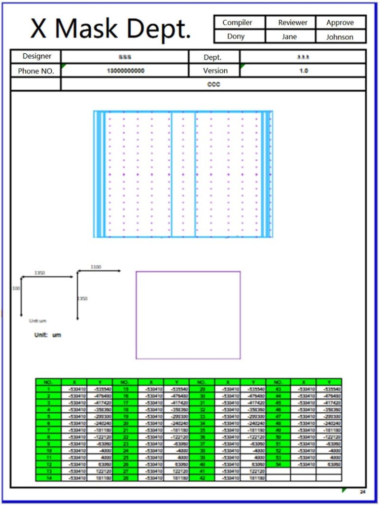
After both the Mask and Glass layouts are completed, the Mark information needs to be extracted to the production department. At this time, the Job File function is required. The Job File function automatically extracts the coordinate list of the specified marks and outputs the process file according to the specified template or rules for the post-layout steps. Generally speaking, the output process file will be used as the reference coordinate file for machine work and other production processes.
Summary
In the three blog series we’ve covered a lot of details on how modern FPD designs can be automated through the successive steps of: circuit schematic, layout, SPICE device modeling, SPICE circuit simulation, RC layout extraction, IR-drop analysis, thermal analysis, design verification and mask analysis.
Empyrean has been focusing on the FPD design automation area since 2012, so give them a call when your team ventures into this product development area. Expect new developments from Empyrean in the area of design kits for OLED and Micro LED devices, and improved optoelectronic hybrid simulation. Going beyond electrical simulation of FPD, there are many areas for expansion.
References
- Carl Ebeling. “Gemini II: A Second Generation Layout Validation Tool”,Proceedings of the IEEE International Conference on Computer Aided Design (ICCAD-88), pp. 322-325, November 1988
- Zhou Peide, “Computational Geometry: Algorithm Design and Analysis”, Tsinghua University Press, 2005
- Thomas H. Cormen, Charles E. Leiserson, “Introduction to Algorithms”, China Machine Press, 2006
- Liu Weiping, Zhou Zhenya, Cai Yici, “A Hybrid Acceleration Algorithm for Post-layout Parallel Circuit Simulation”, Journal of Computer-Aided Design and Graphics Theory, 28(11),2016-2020, 2016
- Yang Liu, “A new generation high performance parallel circuit simulation tool”, China Integrated Circuit, October 2016
- Lifeng Wu, “Enable Full Panel Circuit Simulation to Improve Brightness Uniformity”, Invited Paper, 9th International Conference on CADTFT, ShenZhen, China, November, 2018
- Lifeng Wu, “Exploring New Tides of EDA”, Invited Paper, 25th Asia and South Pacific Design Automation Conference (ASPDAC), Beijing, China, January 2020
- Lu, T., Wang, Z., and Yu, W. “Hierarchical Block Boundary-Element Method (HBBEM): A Fast Field Solver for 3-D Capacitance Extraction.” Microwave Theory & Techniques IEEE Transactions on 52.1:10-19.
- Lu Taotao, Wang Guanghui, Hou Jinsong, Wang Zeyi, “Hierarchical h-Adaptive Computation in VLSI 3-D Capacitance Extraction”, Chinese Journal of Semiconductors, 543-549,2002
- Jinsong Hou,Zeyi Wang,Xianlong Hong,“The hierarchical h-adaptive 3-D boundary element computation of VLSI interconnect capacitance”,ASPDAC,1999
- J. Sun, “IR-drop compensation for large size AMOLED”, IDW Tech. Dig., pp. 183-184, December 2011
Also Read
Curvilinear FPD Layout and Schematics
Automating the Design of Flat Panel Displays
Xilinx Moves from Internal Flow to Commercial Flow for IP Integration
Share this post via:


Comments
There are no comments yet.
You must register or log in to view/post comments.