You are currently viewing SemiWiki as a guest which gives you limited access to the site. To view blog comments and experience other SemiWiki features you must be a registered member. Registration is fast, simple, and absolutely free so please,
join our community today!
WP_Term Object
(
    [term_id] => 158
    [name] => Semiconductor
    [slug] => semiconductor-manufacturers
    [term_group] => 0
    [term_taxonomy_id] => 158
    [taxonomy] => category
    [description] =>
    [parent] => 0
    [count] => 1407
    [filter] => raw
    [cat_ID] => 158
    [category_count] => 1407
    [category_description] =>
    [cat_name] => Semiconductor
    [category_nicename] => semiconductor-manufacturers
    [category_parent] => 0
    [is_post] =>
)
TSMC attends DAC every year and they do something very savvy, it’s a theatre where they invite all of their EDA and IP partners to present something of interest, followed by a drawing for a prize. At the end of the day they even have a nice prize, like a MacBook Air, which I didn’t win. On Wednesday I watched Dave Reed of Synopsys… Read More
Samsung Foundry Update 2019by Tom Dillinger on 06-08-2019 at 5:00 amCategories: Events, FD-SOI, Samsung Foundry
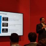
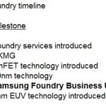
Samsung Foundry recently held their 4th annual technology forum in Santa Clara. This article reviews the highlights of the presentations. There were two prevalent themes throughout – focused execution on the current process roadmap, and the introduction of the 3nm process node features and schedule.
Before getting into … Read More
TSMC, the largest and most influential pure-play foundry, has many fascinating stories to tell. In this section, TSMC covers some of their basic history, and explains how creating an ecosystem of partners has been key to their success, and to the growth of the semiconductor industry.
The history of TSMC and its Open Innovation … Read More
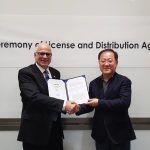
There were quite a few announcements at the Samsung Foundry Forum but my favorite was the IP partnership between Samsung and Silvaco. IP is a critical part of the fabless ecosystem and one of the advantages an IDM foundry has over a pure-play is the vast amounts of internal IP that have been silicon proven over the years. With Samsung… Read More
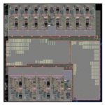
Since the beginning of May eSilicon has announced the tape-out of three TSMC 7nm test chips. The first of these, a 7nm 400G Ethernet Gearbox/Retimer design, caught my eye and I followed up with Hugh Durdan, their vice president of strategy and products, to learn more about it. Rather than just respin their 56G SerDes, they decided… Read More
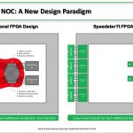
Why does it seem like current FPGA devices work very much like the original telephone systems with exchanges where workers connected calls using cords and plugs? Achronix thinks it is now time to jettison Switch Blocks and adopt a new approach. Their motivation is to improve the suitability of FPGAs to machine learning applications,… Read More
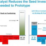
It is said that it will cost as much as $600M to develop a 5nm chip. At that price, only a few companies can afford to play, and with that amount of cash in, innovation is severely limited.
At the same time, there is a stampede in the artificial intelligence (AI) market where around 60 startups have appeared, many of which have already … Read More
Hardware is roaring back into prominence in technology innovation, from advanced cars to robots, smart homes and smart cities, 5G communication and the burgeoning electronification of industry, medicine and utilities. While software continues to play a role, all of these capabilities depend fundamentally on advances in … Read More
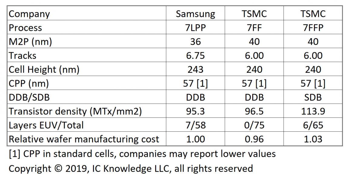
Samsung and TSMC have both made recent disclosures about their 5nm process and I though it would be a good time to look at what we know about them and compare the two processes.
A lot of what has been announced about 5nm is in comparison to 7nm so we will first review 7nm.
7nm
Figure 1 compares Samsung’s 7LPP process to TSMC’s 7FF and 7FFP… Read More
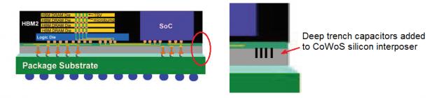
TSMC recently held their annual Technology Symposium in Santa Clara. Part 1 of this article focused on the semiconductor process highlights. This part reviews the advanced packaging technologies presented at the symposium.
TSMC has clearly made a transition from a “pure” wafer-level foundry to a supplier of complex integrated… Read More

Enhancing Multi-Domain System Simulation with FMI Co-Simulation