You are currently viewing SemiWiki as a guest which gives you limited access to the site. To view blog comments and experience other SemiWiki features you must be a registered member. Registration is fast, simple, and absolutely free so please,
join our community today!
WP_Term Object
(
    [term_id] => 158
    [name] => Semiconductor
    [slug] => semiconductor-manufacturers
    [term_group] => 0
    [term_taxonomy_id] => 158
    [taxonomy] => category
    [description] =>
    [parent] => 0
    [count] => 1406
    [filter] => raw
    [cat_ID] => 158
    [category_count] => 1406
    [category_description] =>
    [cat_name] => Semiconductor
    [category_nicename] => semiconductor-manufacturers
    [category_parent] => 0
    [is_post] =>
)
High volume manufacturing is a 24/7 business with 12 hour shifts. You don’t always get to pick the shifts you want and you must cover for others when they can’t. It’s a challenging career and not for the faint of heart like myself.
In the 1980s and 1990s I spent time in Japan working with some of the top Japanese semiconductor manufacturers.… Read More
Japan’s Foundry Morgana Part IIby Karl Breidenbach on 08-10-2023 at 10:00 amCategories: Semiconductor
Japan’s Foundry Morgana: A Journey from Mirage to Reality?Three years ago, I wrote an article about Japan’s semiconductor industry under the title “Japan’s Foundry Morgana.” Back in September 2020, I analyzed the decline of Japan’s once world-leading semiconductor sector and the … Read More
Now that semiconductors are front page news and a political football, I would like to write more about how we got to where we are today to better understand where semiconductors will go tomorrow. I will start this article with a provocative quote that really made me laugh and will put some context to what I am trying to accomplish here:… Read More
The trend is undeniable. Highly integrated monolithic chips can no longer handle the demands of next-generation systems. The reasons for this significant shift in design are many. Much has been written on the topic; you can get a good overview of the forces at play in multi-die design here. These changes represent the next chapter… Read More
For many years, monolithic chips defined semiconductor innovation. New microprocessors defined new markets, as did new graphics processors, and cell-phone chips. Getting to the next node was the goal, and when the foundry shipped a working part victory was declared. As we know, this is changing. Semiconductor innovation is… Read More
On the heels of the TSMC Symposium and the Intel Foundry update, Samsung held their Foundry Forum today live in Silicon Valley. As usual it was a well attended event with hundreds of people and dozens of ecosystem partners. The theme was the AI Era which is appropriate. As I have mentioned before, AI will touch most every chip and there… Read More
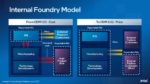
Intel held a webinar today to discuss their IDM2.0 internal foundry model. On the call were Dave Zinsner Executive Vice President and Chief Financial Officer and Jason Grebe Corporate Vice President and General Manager of the Corporate Planning Group.
On a humorous note, the person moderating the attendee questions sounded … Read More
(First published December 24, 2014)
A list of the best and worst CEOs in 2014 was recently published. The good news is that none of our semiconductor CEOs were on the worst list. The bad news is that none of our semiconductor CEOs were on the best list either. I will be writing about the CEOs that made our industry what it is today starting… Read More
Many credible market analysis firms are predicting the semiconductor market to reach the trillion dollar mark over the next six years or so. Just compare this to the more than six decades it took for the market to cross the $500 billion mark. The projected growth rate is incredible indeed and is driven by fast growing market segments… Read More
As one of the world’s leading chip foundries, Samsung occupies a vital position in the semiconductor value chain. The annual Samsung Advanced Foundry Ecosystem (SAFE™) Forum is a must-go event for semiconductor and electronic design automation (EDA) professionals. Ajei Gopal, President and CEO of Ansys, has the honor of delivering… Read More


The Silicon Shield Has Never Been Stronger!