You are currently viewing SemiWiki as a guest which gives you limited access to the site. To view blog comments and experience other SemiWiki features you must be a registered member. Registration is fast, simple, and absolutely free so please,
join our community today!
WP_Term Object
(
    [term_id] => 16126
    [name] => Lithography
    [slug] => lithography
    [term_group] => 0
    [term_taxonomy_id] => 16126
    [taxonomy] => category
    [description] =>
    [parent] => 0
    [count] => 187
    [filter] => raw
    [cat_ID] => 16126
    [category_count] => 187
    [category_description] =>
    [cat_name] => Lithography
    [category_nicename] => lithography
    [category_parent] => 0
    [is_post] =>
)
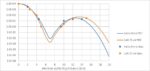
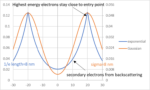
The release and scattering of photoelectrons and secondary electrons in EUV resists has often been glossed over in most studies in EUV lithography, despite being a fundamental factor in the image formation. Fortunately, Intel has provided us with a laboriously simulated electron release and scattering model, using the GEANT4… Read More
In the closing scene of Steven Spielberg’s Raiders of the Lost Ark (1981), the camera pulls back to reveal an enormous warehouse stacked with crates of artifacts hidden away by the US government.
One could imagine a similar warehouse in China today. The crates would hold a different kind of treasure – semiconductor production … Read More
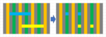
Electron beam lithography is commercially used to directly write submicron patterns onto advanced node masks. With the advent of EUV masks and nanometer-scale NIL (nanoimprint lithography), multi-beam writers are now being used, compensating the ultralow throughput of a single high-resolution electron beam with the use… Read More
- KLA has an OK quarter in an ugly market- bouncing along bottom
- Like Lam & ASML, China was huge at 43% represents more risk
- 2/3 Foundry/logic, 1/3 memory – Process tools were weak
- No change, stable , no visibility on recovery
Quarter and guide were good in continued ugly industry
As expected KLAC reported earnings at the … Read More
- ASML reports in-line QTR but future looks flat for 2024
- Downcycle finally hits litho leader- ASML monopoly solid as ever
- Memory remains bleak – New China sanctions unclear
- Recovery timing is unclear but planning for an up 2025
In Line Quarter and year as expected
Overall revenues came in at Euro6.7B with EPS at Euro4.81, more… Read More
- This past weeks over-reaction to Canon echoes the Sculpta Scare
- Nanoimprint has made huge strides but is still not at all competitive
- Shows basic lack of understanding of technology by some pundits
- Chip industry has been searching for alternatives that don’t exist
Much ado about nothing much…..
This past week we … Read More
– SPIE EUV & Photomask conference well attended with great talks
– Chip industry focused on next gen High NA EUV & what it impacts
– Do big chips=big masks? Another Actinic tool?
– AI & chip tools, a game changer- China pre-empting more sanctions
The SPIE EUV & Photomask conference in Monterey
…
Read More
China’s recent achievement of a 7nm-class foundry node using only DUV lithography [1] raises the question of how far DUV lithography can be extended by multipatterning. A recent publication at CSTIC 2023 indicates that Chinese groups are currently looking at extension of DUV-based multipatterning to 5nm, going so far… Read More
Recent articles have focused much effort on studying the stochastic behavior of secondary electron exposure of EUV resists [1-4]. Here, we consider the implications of extending similar treatments to DUV lithography.
Basic Model Setup
As before, the model uses pixel-by-pixel calculations of absorbed photon dose, followed… Read More
Introduction
The ever-growing demand for faster, smaller, and more efficient electronic devices has fueled the semiconductor industry’s relentless pursuit of innovation. One crucial technology at the heart of semiconductor manufacturing is Extreme Ultraviolet Lithography (EUVL) to achieve smaller feature sizes… Read More


Silicon Insurance: Why eFPGA is Cheaper Than a Respin — and Why It Matters in the Intel 18A Era