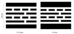
CHERI webinar banner
WP_Term Object
(
    [term_id] => 16126
    [name] => Lithography
    [slug] => lithography
    [term_group] => 0
    [term_taxonomy_id] => 16126
    [taxonomy] => category
    [description] => 
    [parent] => 0
    [count] => 159
    [filter] => raw
    [cat_ID] => 16126
    [category_count] => 159
    [category_description] => 
    [cat_name] => Lithography
    [category_nicename] => lithography
    [category_parent] => 0
    [is_post] => 
)

SPIE 2023 – imec Preparing for High-NA EUV

SPIE 2023 – imec Preparing for High-NA EUV
by Scotten Jones on 05-17-2023 at 6:00 am

Figure 1 Pellicle Transmission

The SPIE Advanced Lithography Conference was held in February. I recently had the opportunity to interview Steven Scheer, vice president of advanced patterning process and materials at imec and review selected papers that imec presented.

I asked Steve what the overarching message was at SPIE this year, he said readiness for … Read More


Curvilinear Mask Patterning for Maximizing Lithography Capability

Curvilinear Mask Patterning for Maximizing Lithography Capability
by Fred Chen on 05-09-2023 at 10:00 am

Curvilinear 1

Masks have always been an essential part of the lithography process in the semiconductor industry. With the smallest printed features already being subwavelength for both DUV and EUV cases at the bleeding edge, mask patterns play a more crucial role than ever. Moreover, in the case of EUV lithography, throughput is a concern, … Read More


Reality Checks for High-NA EUV for 1.x nm Nodes

Reality Checks for High-NA EUV for 1.x nm Nodes
by Fred Chen on 04-26-2023 at 6:00 am

Reality Checks for High NA EUV for 1.x nm Nodes

The “1.xnm” node on most roadmaps to indicate a 16-18 nm metal line pitch [1]. The center-to-center spacing may be expected to be as low as 22-26 nm (sqrt(2) times line pitch). The EXE series of EUV (13.5 nm wavelength) lithography systems from ASML feature a 0.55 “High” NA (numerical aperture), targeted… Read More


LAM Not Yet at Bottom Memory Worsening Down 50%

LAM Not Yet at Bottom Memory Worsening Down 50%
by Robert Maire on 04-24-2023 at 10:00 am

LAM RESEARCH Vantex external chamber lrg 300x300

-Lam reported in line results on reduced expectations
-Guidance disappoints as memory decline continues
-Memory capex down 50% but still sees “further declines”
-Lam ties future to EUV maybe not good idea after ASML report

Lam comes in above grossly already reduced expectations
and misses on guidance

We always … Read More


ASML Wavering- Supports our Concern of Second Leg Down for Semis- False Bottom

ASML Wavering- Supports our Concern of Second Leg Down for Semis- False Bottom
by Robert Maire on 04-21-2023 at 8:00 am

Semiconductor False Bottom

-ASML weakness is evidence of deeper chip down cycle
-When ASML sneezes other chip equip makers catch a cold
-Will backlog last long enough? Will EUV demand hold up?
-“Unthinkable” event, litho cancelations, could shock industry

ASML has in line quarter but alarm bells ring on wavering outlook

ASML reported Euro6.7B… Read More


Can Attenuated Phase-Shift Masks Work For EUV?

Can Attenuated Phase-Shift Masks Work For EUV?
by Fred Chen on 04-18-2023 at 6:00 am

1679926948898

Normalized image log-slope (NILS) is probably the single most essential metric for describing lithographic image quality. It is defined as the slope of the log of intensity, multiplied by the linewidth [1], NILS = d(log I)/dx * w = w/I dI/dx.  Essentially, it gives the % change in width for a given % change in dose. This is particularly… Read More


Lithography Resolution Limits: The Point Spread Function

Lithography Resolution Limits: The Point Spread Function
by Fred Chen on 03-21-2023 at 6:00 am

Lithography Resolution Limits The Point Spread Function

The point spread function is the basic metric defining the resolution of an optical system [1]. A focused spot will have a diameter defined by the Airy disk [2], which is itself a part of the diffraction pattern, based on a Bessel function of the 1st kind and 1st order J1(x), with x being a normalized coordinate defined by pi*radius/(0.5… Read More


Sino Semicap Sanction Screws Snugged- SVB- Aftermath more important than event

Sino Semicap Sanction Screws Snugged- SVB- Aftermath more important than event
by Robert Maire on 03-15-2023 at 10:00 am

China Chip Embargo

-Reports of further tightening of China SemiCap Restrictions
-Likely closing loopholes & pushing back technology line
-Dutch have joined, Japan will too- So far no Chinese reaction
-SVB is toast but repercussions may be far worse

Reports of tightening semiconductor sanctions on Friday

It was reported byBloomberg of Friday… Read More


Resolution vs. Die Size Tradeoff Due to EUV Pupil Rotation

Resolution vs. Die Size Tradeoff Due to EUV Pupil Rotation
by Fred Chen on 03-02-2023 at 10:00 am

Resolution vs. Die Size Tradeoff Due to EUV Pupil Rotation

The many idiosyncrasies of EUV lithography affect the resolution that can actually be realized. One which still does not get as much attention as it should is the cross-slit pupil rotation [1-3]. This is a fundamental consequence of using rotational symmetry in ring-field optical systems to control aberrations in reflective… Read More


KLAC- Weak Guide-2023 will “drift down”-Not just memory weak, China & logic too

KLAC- Weak Guide-2023 will “drift down”-Not just memory weak, China & logic too
by Robert Maire on 02-06-2023 at 6:00 am

KLAC Tencor SemiWiki

-Business will “drift down” over the course of 2023
-Not just memory is weak- China issue, foundry/logic slowing
-March guide worse than expected (Like Lam)
-Backlog likely saw push outs & cancelations but still long

Good quarter but weak guide

Much as we saw with Lam, KLA reported a beat on the December quarter… Read More