You are currently viewing SemiWiki as a guest which gives you limited access to the site. To view blog comments and experience other SemiWiki features you must be a registered member. Registration is fast, simple, and absolutely free so please,
join our community today!
WP_Term Object
(
    [term_id] => 89
    [name] => FinFET
    [slug] => finfet
    [term_group] => 0
    [term_taxonomy_id] => 89
    [taxonomy] => category
    [description] =>
    [parent] => 0
    [count] => 231
    [filter] => raw
    [cat_ID] => 89
    [category_count] => 231
    [category_description] =>
    [cat_name] => FinFET
    [category_nicename] => finfet
    [category_parent] => 0
    [is_post] =>
)
The challenges of 7nm are well documented. Lithography artifacts create exploding design rule complexity, mask costs and cycle time. Noise and crosstalk get harder to deal with, as does timing closure. The types of applications that demand 7nm performance will often introduce HBM memory stacks and 2.5D packaging, and that creates… Read More
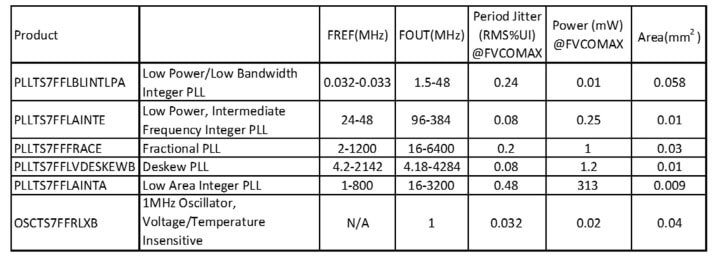
Designing at 7nm is a big deal because of the costs to make masks and then produce silicon that yields at an acceptable level, and Silicon Creations is one company that has the experience in designing AMS IP like: PLL, Serializer-Deserializer, IOs, Oscillators. Why design at 7nm? Lots of reasons – lower power, higher speeds,… Read More
ANSYS and TSMC will be co-presenting at ARM TechCon on Multiphysics Reliability Signoff for Next Generation Automotive Electronics Systems. The event is on Thursday October 26th, 10:30am-11:20am in Grand Ballroom B.
You can get a free Expo pass which will give you access to this event HERE and see the session page for the event … Read More
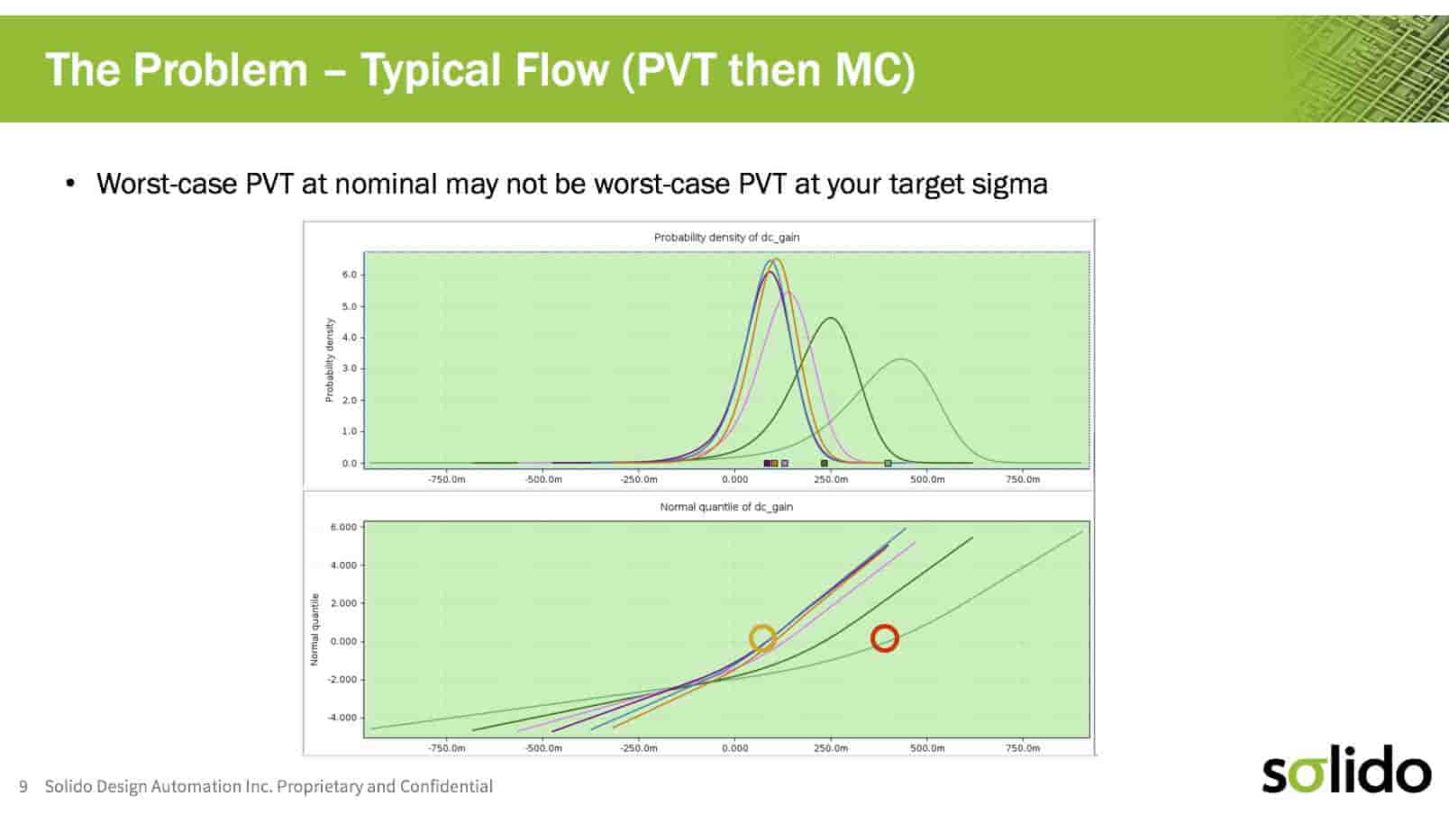
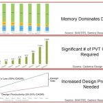
TSMC held its Open Innovation Platform Forum the other week on September 13[SUP]th[/SUP]. Each year the companies that exhibit at this event choose to highlight their latest technology. One of the most interesting presentations that I received during the event was from Solido. In recent years they have produced a number of groundbreaking… Read More
On September 20th GLOBALFOUNDRIES (GF) held their annual technology conference. The conference presented an opportunity to hear the latest on the fascinating journey GF has been on.… Read More
Webinars are a very effective communications channel in a fast paced industry like semiconductor design. If you sign-up in advance and you can’t make the live version, you will be automatically notified when the replay is available so you can watch it at your leisure. I’m guilty of this for sure, because of my hectic… Read More
Open Silicon hosted a webinar today focusing on their High Bandwidth Memory (HBM) IP-subsystem product offering. Their IP-subsystem is based on the HBM2 standard and includes blocks for the memory controller, PHY and high-speed I/Os, all targeted to TSMC 16nm FF+ process. The IP-subsystem supports the full HBM2 standard with… Read More
My IC design career started out with DRAM design, characterization and verification back in the 1970’s, so I vividly recall how much SPICE circuit simulation was involved, and how little automation we had back in the day, so we tended to cobble together our own scripts to help automate the process a bit. With each new process… Read More
In automotive applications, advanced FinFET processes are great for high levels of integration and low power. But they also present some new challenges in reliability signoff. Ansys will be hosting a webinar to highlight the challenges faced by engineers trying to ensure thermal, electromigration (EM) and electrostatic discharge… Read More
One of my favorite classes in college was the lab exercise, mostly because we actually got to use real electronics and then measure something, finally writing it up in our lab notebooks. The issue today is that a college student taking Electrical Engineering probably doesn’t have much access to 10nm FinFET silicon for use… Read More


Musk’s Orbital Compute Vision: TERAFAB and the End of the Terrestrial Data Center