You are currently viewing SemiWiki as a guest which gives you limited access to the site. To view blog comments and experience other SemiWiki features you must be a registered member. Registration is fast, simple, and absolutely free so please,
join our community today!
WP_Term Object
(
    [term_id] => 50
    [name] => Events
    [slug] => events
    [term_group] => 0
    [term_taxonomy_id] => 50
    [taxonomy] => category
    [description] =>
    [parent] => 0
    [count] => 1564
    [filter] => raw
    [cat_ID] => 50
    [category_count] => 1564
    [category_description] =>
    [cat_name] => Events
    [category_nicename] => events
    [category_parent] => 0
    [is_post] =>
)
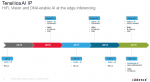
This blog is my second blog from this year’s Linley Fall Processor Conference. The first two blogs focused on edge inference solutions. Achronix’s discussion was much broader than just AI/ML; it was about where FPGA’s have been going and culminated with a product announcement preview. I’ll get to the announcement in a moment, … Read More
Bob Swan started as interim CEO in June of 2018 and took the full-time CEO job in January of 2019. I was a vocal critic of the previous CEO Brian Krzanich (BK) and really felt he was not fit to serve. As it turns out I was right. It is not just the CEO himself, but also the people that he surrounds himself with. BK surrounded himself with the… Read More
Last week I attended the Linley Fall Processor Conference held in Santa Clara, CA. This blog is the first of three blogs I will be writing based on things I saw and heard at the event.
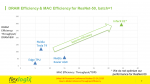
In April, Flex Logix announced its InferX X1 edge inference co-processor. At that time, Flex Logix announced that the IP would be available and that a chip,… Read More
Connecting the Divide between Design and Manufacturing is an overarching theme within the ESD Alliance as these two essential semiconductor disciples become more reliant on each other. It’s also the reason we’re hosting SMART Design, the first system-centric series showcasing advances in electronic system design to be held… Read More
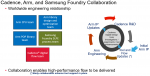
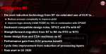
In a joint presentation given by Samsung, Arm, and Cadence at the Arm TechCon event on October 9, 2019, Cadence showed some results and explained its collaboration project used to implement the new Arm Hercules CPU on Samsung’s advanced 5LPE process. I do not want to minimize the significance of Samsung’s and Arm’s participation… Read More
My first DAC was in 1987 so I’ve seen our industry expand greatly over the years, and I expect that #57DAC on July 19-23, 2020 in SFO to be another exciting event to attend for semiconductor professionals from around the globe. What makes DAC so compelling for me to visit are the people, exhibitors, panel discussions, technical… Read More
This will be a combination of the recent TSMC quarterly report, a look back at Cliff Hou’s keynote at the most recent TSMC conference, and conversations on SemiWiki.com. There has been a lot of press on this but of course the most important points are being missed. Semiconductors are complicated and getting more so, absolutely.… Read More
In September, ClioSoft gave a SemiWiki webinar titled, Reusing Your IPs & PDKs Successfully With Cadence® Virtuoso®. I was happy to be the moderator of this webinar, having had the chance to work with ClioSoft’s team over many years. The webinar was informative while also being very time efficient. I think it is important for… Read More
There are some metaphorical similarities between reaching timing signoff and driving a car to your destination. Most of us get in the car, turn the key and push the gas pedal to make it go. While we might have a cursory understanding of what makes it go, there are actually a lot of “moving part” under the hood in each instance. For most… Read More


TSMC CoWoS versus Intel EMIB Semiconductor Packaging