You are currently viewing SemiWiki as a guest which gives you limited access to the site. To view blog comments and experience other SemiWiki features you must be a registered member. Registration is fast, simple, and absolutely free so please,
join our community today!
            WP_Term Object
(
    [term_id] => 14
    [name] => Synopsys
    [slug] => synopsys
    [term_group] => 0
    [term_taxonomy_id] => 14
    [taxonomy] => category
    [description] =>
    [parent] => 157
    [count] => 784
    [filter] => raw
    [cat_ID] => 14
    [category_count] => 784
    [category_description] =>
    [cat_name] => Synopsys
    [category_nicename] => synopsys
    [category_parent] => 157
    [is_post] =>
)

WP_Term Object
(
    [term_id] => 14
    [name] => Synopsys
    [slug] => synopsys
    [term_group] => 0
    [term_taxonomy_id] => 14
    [taxonomy] => category
    [description] =>
    [parent] => 157
    [count] => 784
    [filter] => raw
    [cat_ID] => 14
    [category_count] => 784
    [category_description] =>
    [cat_name] => Synopsys
    [category_nicename] => synopsys
    [category_parent] => 157
    [is_post] =>
)
Usually, we get the incremental story in news: this new release is x percent better at this or that than the previous release, and so on. Often missing is the big picture, telling how the pieces all tie together. Synopsys took on that challenge in their latest FPGA-based prototyping webinar. … Read More
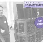
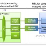
Hybrid Emulationby Paul McLellan on 07-25-2014 at 9:01 amCategories: EDA, Synopsys
Hybrid emulation is when part of the system is run in the emulator and part of the system is run in a virtual prototype. Typically a model of the processor(s) is run in the virtual platform and then the rest of the design is modeled by running the RTL on the emulator. I talked to Tom Borgstrom at Synopsys about what technology they have … Read More
Test engineers are often the unsung heroes in the semiconductor world, because they have the tough job of deciding if each IC is good or bad, while taking the least amount of time on a tester and ensuring that the tests are actually finding and uncovering all manufacturing and process variation defects. Simple stuck-at fault models… Read More
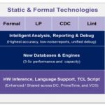
Synopsys announced verification compiler a couple of months ago and dropped hints about their static and formal verification. They haven’t announced anything much for a couple of years and it turns out that the reason was that they decided that the technology that they had, some internally developed and some acquired, … Read More
During my illustrious career one of the most useful axioms that I use just about everyday day is: “Understand what people say but also understand why they are saying it.” This certainly applies to press releases so let’s take a look at what Intel unleashed during #51DAC (in alphabetical order):
ANSYS And Intel Collaborate… Read More
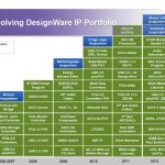
Synopsys has been extremely active, during the last 10 years, not only launching new IP products every year, but also running an ambitious acquisition strategy, with no less than 8 acquisitions. Cascade acquisition bring PCI Express (controller only), when Accelerant bring SerDes (the earth of any PHY IP). The MIPS/Chipidea… Read More
This is a new brick that Synopsys brings to build FD-SOI credibility. We have talked at Semiwiki about FD-SOI technology developed by the LETI and STM, and recently endorsed by Samsung Foundry, offering a more than credible second source to STM. And we have said that the FD-SOI introduction will need to be supported by EDA and IP vendors… Read More
How much power does a system consume? The simplistic path to power estimation for a system used to be tossing a few metrics – standby, typical, worst case, with figures pulled from a datasheet, simulation, or physical measurement – into a spreadsheet. After filling the remaining holes with SWAG (scientific wild-ass guesses), … Read More
Tuesday morning at DAC I enjoyed a free breakfast courtesy of Synopsysand GLOBALFOUNDRIESwhere I learned more about the emerging market of IoT, and what it means to semiconductor, EDA and IP vendors. Panelists included: Semico Research, HP, Synopsys, GLOBALFOUNDRIES and Broadcom. … Read More
Synopsyshosted an AMS Luncheon panel today at DACin the Westin Hotel and invited four customers to talk about their actual design challenges and experiences. I’ve typed up my notes from this event.… Read More