As a professional conference goer I can see definite trends when it comes to topics and attendance. Thus far this year I have seen a double digit increase in attendance, which is great. The question is why? Why is the fabless semiconductor ecosystem leaving the safety of their cubicles and computer screens in droves to mingle amongst… Read More

Electronic Design Automation
US is the Ultimate Leader in Semiconductor Business
Last year in November when I looked at the world’s top20 semiconductor companies with Samsungand TSMCbeing at the second and third rank respectively, first being Intel, I computed the sales numbers of the companies based on their countries and found that Taiwan and South Korea accounted for 34.5% of the total sales of the top20 … Read More
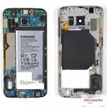
What is Inside of the Samsung Galaxy S6?
I’ve always been curious about what is inside an electronic device, and it was seeing the very first TI handheld calculator that got me started into a career as an Electrical Engineer. Next to Apple, the most popular brand in smart phone devices these days has got to be Samsung and they have just launched the Galaxy S6 device.… Read More
Security All Around in SoCs at DAC
Last month I was on my way to write a detailed article on important aspects to look at while designing an SoC. This was important in the new context of modern SoCs that go much beyond the traditional power, performance and area (PPA) requirements. I had about 12-13 parameters in my list that I couldn’t cover in one go, so I put the write-up… Read More
The Changing Foundry Landscape: Trends and Challenges!
This will be a year of change for the fabless semiconductor ecosystem, absolutely. Last year we were wondering how Samsung Mobile was going to compete with the China clones and other low end smart phones. We now know the answer to that question thanks to the Chipworks tear down of the Galaxy S6. SemiWiki IP expert Dr. Eric Esteve blogged… Read More
Variation Alphabet Soup

On-chip variation (OCV) is a major issue in timing signoff, especially at low voltages or in 20/16/14nm processes. For example, the graph below shows a 20nm inverter. At 0.6V the inverter has a delay of 2 (nominalized) units. But due to on-chip variation this might be as low as 1.5 units or as high as 3 units, which is a difference from… Read More
DAC Keynotes: Mark Your Calendar
DAC starts in San Francisco on June 8th. The kickoff keynote at 9.20am that morning is by Brian Otis of Google. He is a director at Google[x]. According to Wikipedia:Google X, stylized as Google[x], is a semi-secret facility run by Google dedicated to making major technological advancements. It is located about a half mile from … Read More
ANSYS Event to Highlight Cutting Edge Technology Development

If you follow technology news, it would be hard to deny that we live in exciting times. In some ways there is an unparalleled amount of big and cool technology development going on right now. We all have followed the rise of Tesla Motors. They took over a long vacant US big-auto plant in Fremont and are reinventing the US automobile industry.… Read More
EDPS: Fins and FinFETs
Look at those dolphins with fins on their backs. Did you know that FinFETs are actually named after them since Chenming Hu and his team though that they looked like a fish’s fin? And since they invented FinFETs they got to name them too. But those dolphins also mean that it is nearly time for this years Electronic Design Process… Read More
What is Skipper?

What is Skipper? Well, it seems it’s a penguin in the movie Madagascar. And one of Barbie’s sisters. Who knew? But for Semiwiki readers it’s an integrated chip finishing platform from ICScape. Skipper can read in full-chip layout extremely fast, examine it and manipulate it in various ways, and write it out again.… Read More
Silicon Insurance: Why eFPGA is Cheaper Than a Respin — and Why It Matters in the Intel 18A Era