You are currently viewing SemiWiki as a guest which gives you limited access to the site. To view blog comments and experience other SemiWiki features you must be a registered member. Registration is fast, simple, and absolutely free so please,
join our community today!
All-Digital In-Memory Computingby Tom Dillinger on 03-15-2021 at 6:00 amCategories: Events, Foundries, TSMC
Research pursuing in-memory computing architectures is extremely active. At the recent International Solid State Circuits conference (ISSCC 2021), multiple technical sessions were dedicated to novel memory array technologies to support the computational demand of machine learning algorithms.
The inefficiencies associated… Read More
Register File Design at the 5nm Nodeby Tom Dillinger on 03-10-2021 at 2:00 pmCategories: Events, Foundries, TSMC
“What are the tradeoffs when designing a register file?” Engineering graduates pursuing a career in microelectronics might expect to be asked this question during a job interview. (I was.)
On the surface, one might reply, “Well, a register file is just like any other memory array – address inputs, data inputs and outputs, read/write… Read More
At the recent ISSCC conference, Mozhgan Mansuri from Intel gave an enlightening (extended) short course presentation on all thing related to clocking, for both wireline and wireless interface design. [1] The presentation was extremely thorough, ranging from a review of basic clocking principles to unique circuit design … Read More
The emergence of advanced packaging technologies has led to the introduction of new types of data communication interfaces. There are a number of topologies that are defined by the IEEE 802.3 standard, as well as the Optical Internetworking Common Electrical I/O CEI standard. [1,2] (Many of the configurations of interest … Read More
Resistive RAM (ReRAM) technology has emerged as an attractive alternative to embedded flash memory storage at advanced nodes. Indeed, multiple foundries are offering ReRAM IP arrays at 40nm nodes, and below.
ReRAM has very attractive characteristics, with one significant limitation:
- nonvolatile
- long retention time
- extremely
…
Read More
With the increasing density of electronics in product enclosures, combined with a broad range of operating frequencies, designers must be cognizant of the issues associated with the radiation and coupling of electromagnetic energy. The interference between different elements of the design may result in coupling noise-induced… Read More
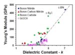
Of the three types of materials used in microelectronics – i.e., semiconductors, metals, and dielectrics – the first two often get the most attention. Yet, there is a pressing need for a rich variety of dielectric materials in device fabrication and interconnect isolation to satisfy the performance, power, and reliability … Read More
Spin-transfer torque magnetoresistive RAM (STT-MRAM) has emerged from several foundries as a very attractive IP option. An introduction to MRAM technology from GLOBALFOUNDRIES was provided in this earlier SemiWiki article. [1]
Briefly, STT-MRAM is a non-volatile storage option with the following attractive characteristics… Read More
The next transition from current FinFET devices at advanced process nodes is the “nanosheet” device, as depicted in the figure below. [1]
The FinFET provides improved gate-to-channel electrostatic control compared to a planar device, where the gate traverses three sides of the fin. The “gate-all-around” characteristics… Read More
What Might the “1nm Node” Look Like?by Tom Dillinger on 12-28-2020 at 6:00 amCategories: EDA, Events, Synopsys
The device roadmap for the next few advanced process nodes seems relatively clear. The FinFET topology will subsequently be displaced by a “gate-all-around” device, typically using multiple stacked channels with a metal gate completely surrounding the “nanosheets”. Whereas the fin demonstrates improved gate-to-channel… Read More








Musk’s Orbital Compute Vision: TERAFAB and the End of the Terrestrial Data Center