Research pursuing in-memory computing architectures is extremely active. At the recent International Solid State Circuits conference (ISSCC 2021), multiple technical sessions were dedicated to novel memory array technologies to support the computational demand of machine learning algorithms.
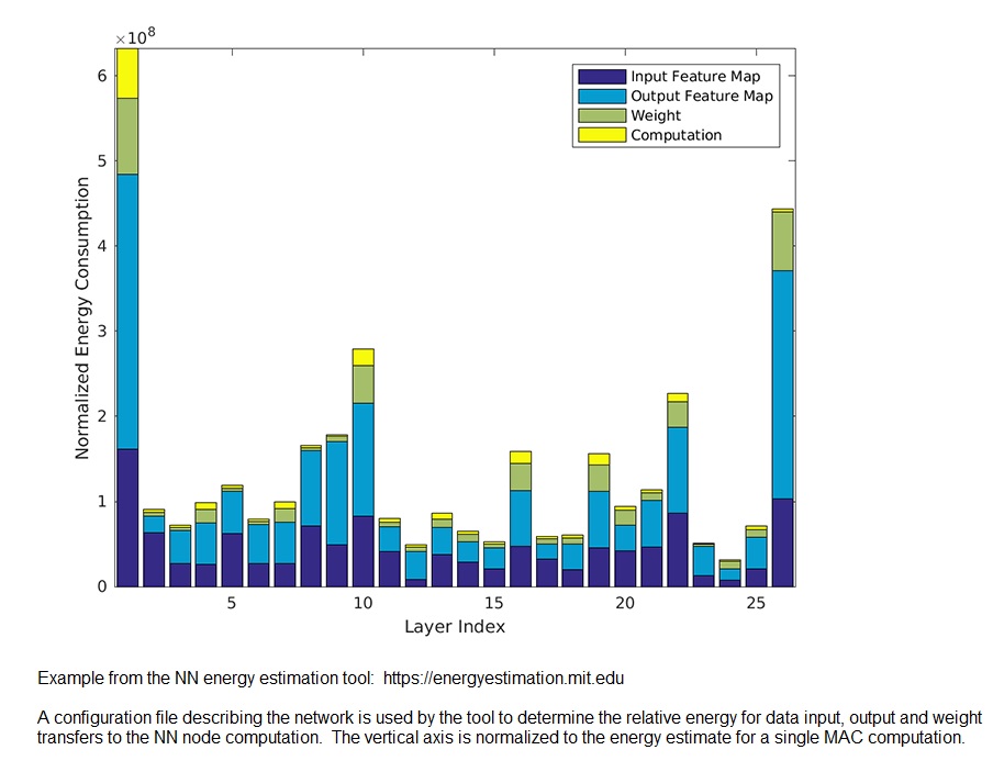
The inefficiencies associated with moving data and weight values from memory to a processing unit, then storing intermediate results back to memory are great. The information transfer not only adds to the computational latency, but the associated power dissipation is a major issue. The “no value add” data movement is a significant percentage of the dissipated energy, potentially even greater than for the “value add” computation, as illustrated below. [1] Note that the actual computational energy dissipation is a small fraction of the energy associated with data and weight transfer to the computation unit. The goal of in-memory computing is to reduce these inefficiencies, especially critical for the implementation of machine learning inference systems at the edge.
The primary focus of in-memory computing for machine learning applications is to optimize the vector multiply-accumulate (MAC) operation associated with each neural network node. The figure below illustrates the calculation for the (trained) network – the product of each data input times weight value is summed, then provided to a bias and activation function.
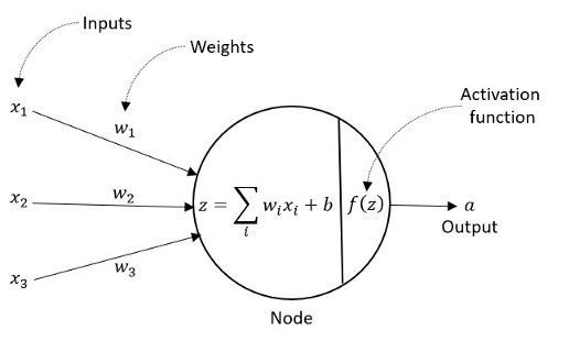
For a general network, the data and weights are typically multi-bit quantities. The weight vector (for a trained, edge AI network) could use a signed, unsigned, or twos complement integer bit representation. For in-memory computing, the final MAC output is realized by the addition of partial multiplication products. The bit width of each (data * weight) arc into the node is well-defined – e.g., the product of 2 n-bit unsigned integers is covered by a 2n-bit vector. Yet, the accumulation of (data * weight) products for all arcs into a highly-connected network could require significantly more bits to accurately represent the MAC result.
One area of emphasis of the in-memory computing research has been to implement a bitline current-sense measurement using resistive RAM (ReRAM) bitcells. The product of the data input (as the active memory row wordline) and weight value stored in the ReRAM cell generates a distinguishable bitline current applied to charge a reference capacitance. A subsequent analog-to-digital converter (ADC) translates this capacitor voltage into the equivalent binary value for subsequent MAC shift-add accumulation. Although the ReRAM-based implementation of the (data * weight) product is area-efficient, it also has its drawbacks:
- the accuracy of the analog bitline current sense and ADC is limited, due to limited voltage range, noise, and PVT variations
- the write cycle time for the ReRAM array is long
- the endurance of the ReRAM array severely limits the applicability as a general memory storage array
These issues all lead to the same conclusion. For a relatively small inference neural network, where all the weights can be loaded in the memory array, and the data vector representation is limited – e.g., 8 bits or less – a ReRAM-based implementation will offer area benefits.
However, for a machine learning application requiring a network larger than stored in the array and/or a workload requiring reconfigurability, updating weight values frequently precludes the use of a ReRAM current sense approach. The same issue applies where the data precision requirements are high, necessitating a larger input vector.
An alternative for an in-memory computing architecture is to utilize an enhanced SRAM array to support (data * weight) computation, rather than a novel memory technology. This allows a much richer set of machine learning networks to be supported. If the number of layers is large, the input and weight values can be loaded into the SRAM array for node computation, output values saved, and subsequent layer values retrieved. The energy dissipation associated with the data and weight transfers is reduced over a general-purpose computing solution, and the issue with ReRAM endurance is eliminated.
In-Memory Computing using an Extended SRAM Design
At the recent ISSCC, researchers from TSMC presented a modified digital-based SRAM design for in-memory computing, supporting larger neural networks.[2]
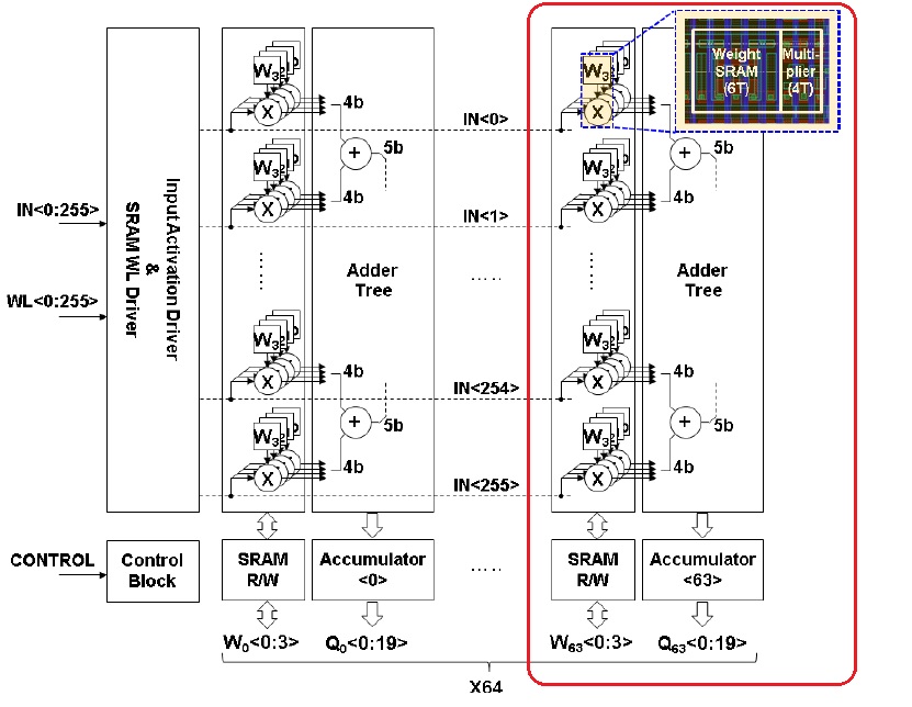
The figure above illustrates the extended SRAM array configuration used by TSMC for their test vehicle – a slice of the array is circled. Each slice has 256 data inputs, which connect to the ‘X’ logic (more on this logic shortly). Consecutive bits of the data input vector are provided in successive clock cycles to the ‘X’ gate. Each slice stores 256 4-bit weight segments, one weight nibble per data input; these weights bits use conventional SRAM cells, as they could be updated frequently. The value stored in each weight bit connects to the other input of the ‘X’ logic.
The figure below illustrates how this logic is integrated into the SRAM.
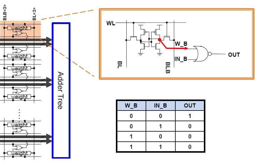
The ‘X’ is a 2-input NOR gate, with a data input and a weight bit as inputs. (The multiplicative product of two one-bit values is realized by an AND gate; by using inverted signal values and DeMorgan’s Theorem, the 2-input NOR gate is both area- and power-efficient.) Between each slice, an adder tree plus partial sum accumulator logic is integrated, as illustrated below.
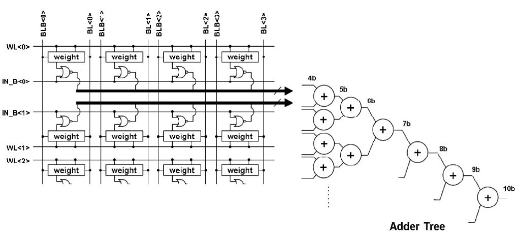
Note that the weight bit storage in the figure above uses a conventional SRAM topology – the weight bit word lines and bit lines are connected as usual, for a 6T bitcell. The stored value at each cell fans out to one input of the NOR gate.
The output of each slice represents a partial product and sum for a nibble of each weight vector. Additional logic outside the extended array provides shift-and-add computations, to enable wider weight value representations. For example, a (signed or unsigned integer) 16-bit weight would combine the accumulator results from four slices.
Testsite results
A micrograph of the TSMC all-digital SRAM-based test vehicle is shown below, highlighting the 256-input, 16 slice (4-bit weight nibble) macro design.
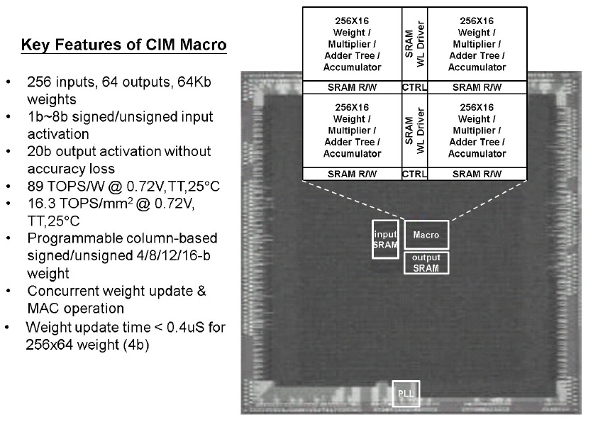
Note that one of the key specifications for the SRAM-based Compute-in-Memory macro is the efficiency with which new weights can be updated in the array.
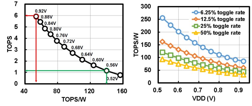
The measured performance (TOPS) and power efficiency (TOPS/W) versus supply voltage are illustrated below. Note that the use of a digital logic-based MAC provides functionality over a wide range of supply voltage.
(Parenthetically, the TOPS/W figure-of-merit commonly used to describe the power efficiency of a neural network implementation can be a misleading measure – it is strongly dependent upon the “density” of the weights in the array, and the toggle rate of the data inputs. There is also a figure below that illustrates how this measure depends upon the input toggle rate, assuming a 50% ratio of ‘1’ values in the weight vectors.)
Although this in-memory computing testsite was fabricated in an older 22nm process, the TSMC researchers provided preliminary area and power efficiency estimates when extending this design to the 5nm node.
Summary
There is a great deal of research activity underway to support in-memory computing for machine learning, to reduce the inefficiencies of data transfer in von Neumann architectures. One facet of the research is seeking to use new memory storage technology, such as ReRAM. The limited endurance of ReRAM limits the scope of this approach to applications where weight values will not be updated frequently. The limited accuracy of bitline current sense also constrains the data input vector width.
TSMC has demonstrated how a conventional SRAM array could be extended to support in-memory computing, for large and/or reconfigurable networks, with frequent writes of weight values. The insertion of 2-input NOR gates and adder tree logic among the SRAM rows and columns provides an area- and power-efficient approach.
-chipguy
References
[1] https://energyestimation.mit.edu
[2] Chih, Yu-Der, et al., “An 89TOPS/W and 16.3TOPS/mm**2 All-Digital SRAM-Based Full-Precision Compute-in-Memory Macro in 22nm for Machine-Learning Applications”, ISSCC 2021, paper 16.4.
Share this post via:


Comments
2 Replies to “All-Digital In-Memory Computing”
You must register or log in to view/post comments.