You are currently viewing SemiWiki as a guest which gives you limited access to the site. To view blog comments and experience other SemiWiki features you must be a registered member. Registration is fast, simple, and absolutely free so please,
join our community today!
The EDA tools industry relies upon ongoing productivity enhancements to existing products, to manage increasing SoC complexity and to address shrinking design schedules. The source of ideas for enhancements can come from a variety of sources – e.g., customer feedback, collaboration with the foundries, and features found … Read More
A significant shift is underway in the fabless semiconductor business model. As the application markets have become more diverse (and more cost-sensitive), product requirements have necessitated a new focus on multi-die packaging technology. … Read More
The EDA tool offerings for printed circuit board design commonly address one of three customer markets: (1) the enterprise design team, (2) the product development engineer, and (3) the “maker”. … Read More
An increasing percentage of SoC die area is being allocated to memory arrays, as applications require more data/instruction storage and boot firmware. Indeed, foundries invest considerable R&D resources into optimizing their array technology IP offerings, often with more aggressive device features than used for other… Read More
High Level Synthesis Updateby Tom Dillinger on 06-29-2016 at 7:00 amCategories: EDA, Siemens EDA
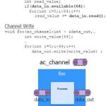
High-level synthesis (HLS) involves the generation of an RTL hardware model from a C/C++/SystemC description. The C code is typically referred to as abehavioraloralgorithmicmodel. The C language constructs and semantics available to architects enable efficient and concise coding – the code itself is smaller, easier to write/read,… Read More
Amidst all the active news about new process introductions at 16/14/10/7nm and the status of next-generation lithography development, there was a recent press release that could have as large an impact upon the microelectronics industry in the United States. A groundbreaking ceremony was recently held in Marcy, New York for… Read More
Top Ten #53DAC Highlightsby Tom Dillinger on 06-13-2016 at 12:00 pmCategories: EDA, Events
Here is a very subjective list of the Top 10 logistical and technical highlights from DAC’53.
(10) With DAC attendance down from its peak days, the Austin Convention Center served as an excellent venue. There was good participation from companies with design centers in the “Silicon Hills”. And, I saw colleagues from Silicon Valley,… Read More
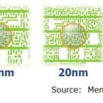
It is truly amazing to consider the advances in microelectronic process development, using 193i photolithography. The figure below is a stark reminder of the difference between the illuminating wavelength and the final imaged geometries. This technology evolution has been enabled by continued investment in mask data generation… Read More
A common SoC design methodology in current use starts with preparation of the physical floorplan — e.g., block/pin placement, global clock domain and bus signal planning, developing the global/local power distribution (and dynamic power domain management techniques). Decoupling capacitor estimated densities and… Read More
There’s an old adage, attributed to renowned computer scientist Andrew Tannenbaum, one that perhaps only engineers find amusing: “The nice thing about standards is that you have so many to choose from.” Nevertheless, IEEE standards arise from customer requirements in the electronics industry. Many relate… Read More


Agentic AI Demands More Than GPUs