You are currently viewing SemiWiki as a guest which gives you limited access to the site. To view blog comments and experience other SemiWiki features you must be a registered member. Registration is fast, simple, and absolutely free so please,
join our community today!
Avionics and Embedded FPGA IPby Tom Dillinger on 10-15-2018 at 12:00 pmCategories: eFPGA, Flex Logix, FPGA, IP
The design of electronic systems for aerospace applications shares many of the same constraints as apply to consumer products – e.g., cost (including NRE), power dissipation, size, time-to-market. Both market segments are driven to leverage the integration benefits of process scaling. … Read More
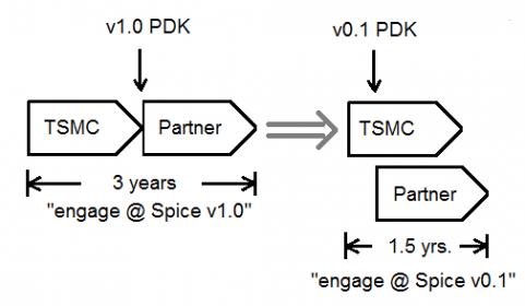
Each year, TSMC hosts two major events for customers – the Technology Symposium in the spring, and the Open Innovation Platform Ecosystem Forum in the fall. The Technology Symposium provides updates from TSMC on:
… Read More
The traditional metrics for evaluating IP are performance, power, and area, commonly abbreviated as PPA. Viewed independently, PPA measures can be difficult to assess. As an example, design constraints that are purely based on performance, without concern for the associated power dissipation and circuit area, are increasingly… Read More
Designers require comprehensive logical, physical, and electrical models to interpret the results of full-chip power noise and electromigration analysis flows, and subsequently deduce the appropriate design updates to address any analysis issues. These models include: LEF, DEF, Liberty library models (including detailed… Read More
An update on the Design Productivity Gapby Tom Dillinger on 08-03-2018 at 12:00 pmCategories: Cadence, EDA
Over a decade ago, a group of semiconductor industry experts published a landmark paper as part of the periodic updates to the International Technology Roadmap for Semiconductors, or ITRS for short (link). The ITRS identified a critical design productivity gap. The circuit capacity afforded by the Moore’s Law pace of technology… Read More
With the increasing complexity and diversity of the mechanical constraints and electrical requirements in electronic product development, printed circuit board designers are faced with a number of difficult challenges:
- generating accurate (S-parameter) simulation models for critical interface elements of the design
…
Read More
At the Design Automation Conference, no one is busier than an EDA company executive — conference panels, product launch briefings, customer meetings, and corporate dinners all place considerable demands on their time. I was fortunate enough to be able to meet with Anirudh Devgan, President of Cadence, at the recent DAC55 in San… Read More
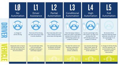
Autonomous Driving and Functional Safetyby Tom Dillinger on 07-25-2018 at 12:00 pmCategories: EDA, Siemens EDA
The timelines proposed by automobile manufacturers for enabling fully autonomous driving are extremely aggressive. At the recent DAC55 conference in San Francisco, I attended a panel discussion on Functional Safety issues for assisted and autonomous driving, sponsored by Mentor Graphics. I also had the opportunity to chat… Read More
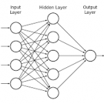
Machine Learning and Embedded FPGA IPby Tom Dillinger on 07-18-2018 at 12:00 pmCategories: eFPGA, Flex Logix, FPGA, IP
Machine learning-based applications have become prevalent across consumer, medical, and automotive markets. Still, the underlying architecture(s) and implementations are evolving rapidly, to best fit the throughput, latency, and power efficiency requirements of an ever increasing application space. Although ML is … Read More
Samsung Foundry recently held their annual technology forum in Santa Clara CA. The forum consisted of: presentations on advanced and mainstream process technology roadmaps; the IP readiness for those technology nodes; a review of several unique package offerings; and, an informal panel discussion with IP designers and EDA… Read More


TSMC CoWoS versus Intel EMIB Semiconductor Packaging